Showing posts with label simple. Show all posts

Thursday, November 6, 2014

Simple Electrification Unit

The circuit is intended for carrying out harmless experiments with high-voltage pulses and functions in a similar way as an electrified fence generator. The p.r.f. (pulse repetition frequency) is determined by the time constant of network R1-C3 in the feedback loop of op amp IC1a: with values as specified, it is about 0.5 Hz. The stage following the op amp, IC1b, converts the rectangular signal into narrow pulses. Differentiating network R2-C4, in conjunction with the switching threshold of the Schmitt trigger inputs of IC1b, determines the pulse period, which here is about 1.5 ms. The output of IC1b is linked directly to the gate of thyristor THR1, so that this device is triggered by the pulses.

The requisite high voltage is generated with the aid of a small mains transformer, whose secondary winding is here used as the primary. This winding, in conjunction with C2, forms a resonant circuit. Capacitor C3 is charged to the supply voltage (12 V) via R3.When a pulse output by IC1b triggers the thyristor, the capacitor is discharged via the secondary winding. The energy stored in the capacitor is, however, not lost, but is stored in the magnetic field produced by the transformer when current flows through it. When the capacitor is discharged, the current ceases, whereupon the magnetic field collapses. This induces a counter e.m.f. in the transformer winding which opposes the voltage earlier applied to the transformer.

Circuit diagram:
Simple Electrification Unit Circuit Diagram

This means that the direction of the current remains the same. However, capacitor C2 is now charged in the opposite sense, so that the potential across it is negative. When the magnetic field of the transformer has returned the stored energy to the capacitor, the direction of the current reverses, and the negatively charged capacitor is discharged via D1 and the secondary winding of the transformer. As soon as the capacitor begins to be discharged, there is no current through the thyristor, which therefore switches off. When C2 is discharged further, diode D1 is reverse-biased, so that the current loop to the transformer is broken, whereupon the capacitor is charged to 12 V again via R3. At the next pulse from IC1b, this process repeats itself.

Since the transformer after each discharge of the capacitor at its primary induces not only a primary, but also a secondary voltage, each triggering of the thyristor causes two closely spaced voltage pulses of opposite polarity. These induced voltages at the secondary, that is, the 230 V, winding, of the transformer are, owing to the higher turns ratio, much higher than those at the primary side and may reach several hundred volts. However, since the energy stored in capacitor C2 is relatively small (the current drain is only about 2 mA), the output voltage cannot harm man or animal. It is sufficient, however, to cause a clearly discernible muscle convulsion.
Read More..

Thursday, October 16, 2014

Simple 150W Amplifier Circuit Diagram

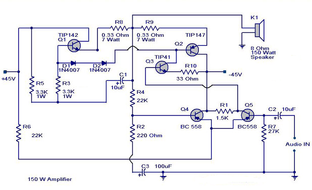
This is the cheapest 150 Watt amplifier circuit you can make,I think.Based on two Darlington power transistors TIP 142 and TIP 147 ,this circuit can deliver a blasting 150 W Rms to a 4 Ohm speaker.Enough for you to get rocked?;then try out this.

TIP 147 and 142 are complementary Darlington pair transistors which can handle 5 A current and 100V ,famous for their ruggedness. Here two BC 558 transistors Q5 and Q4 are wired as pre amplifier and TIP 142 ,TIP 147 together with TIP41  (Q1,Q2,Q3) is used for driving the speaker.This circuit is designed so rugged that this can be assembled even on a perf board or even by pin to pin soldering.The circuit can be powered from a +/-45V, 5A  dual power supply.You must try this circuit.Its working great!

The preamplifier section of this circuit is based around Q4 and Q5 which forms a differential amplifier. The use of a differential amplifier in the input stage reduces noise and also provides a means for applying negative feedback. Thus overall performance of the amplifier is improved. Input signal is applied to the base of Q5 through the DC decoupling capacitor C2. Feedback voltage is applied to the base of Q4 from the junction of 0.33 ohm resistors through the 22K resistor. A complementary Class AB push-pull stage is built around the transistors Q1 and Q2 for driving the loud speaker. Diodes D1 and D2 biases the complementary pair and ensures Class AB operation. Transistor Q3 drives the push-pull pair and its base is directly coupled to the collector of Q5.

 150W Amplifier Circuit Diagram

 150w amplifier circuit diagram

Notes.

  • Remember TIP 142 and 147 are Darlington pairs  .They are shown as conventional transistors in figure for ease.So don’t get confused.Even though each of them have 2 transistors ,2 resistors and 1 diode inside ,only three pins ,base emitter and collector are coming out.Rest are connected internally.So its quite OK to assume each of them as transistor for ease.
  • Use a well regulated and filtered power supply.
  • Connect a 10K POT in series with the input as volume control if you need.Not shown in circuit diagram.
  • All electrolytic capacitors must be rated at least 50volts.

Power supply for this circuit.

A  +40/-40 unregulated dual supply for powering this amplifier project is shown below.  This power supply is only enough for powering one channel and for stereo applications double the current ratings of  the transformer, diodes and fuses.


Read More..

Wednesday, October 15, 2014

Simple DPA 220 schematic


T1 to T6 create the input differential stage. The D7 and D8 zener diodes stabilize at 5V. These are just the simplest low-power zeners, only they have to be coupled in tolerance of 200 milivolts, which should not be a problem. T1 to T6 are common all-purpose low-power transistors with high Hfe. These six and maybe the next four have to be coupled in tolerance of 25%.

The T7 and T8 are fast, switching application types.

T9 and T10 have to be fast and must hold a high voltage, thus the best are the "video" types - BF469/470. T15 and T16 are the same types.

The C9, C10 and C15 should stand voltages higher than usual 50 V - I dont know why.

D3 to D6 can be any silicon type, not Scottky, the ones listed below are just all-purpose low-current ones for 150 V. These diodes should be rather fast - "switching types".

The T11 and T12 stabilize the BIAS current for the power stage. T11 also serves as a temperature sensor, and is mounted to the cooler of power transistors.

T13 and T14 secure the output current - in cooperation with R38 and R39.

The output transistors used here are Tesla types - Tesla is a former local devices manufacturer - the pair in each branch can be replaced with a single power darlington, like BD649/BD650. They should have Pc > 150W, Ic > 15A, Uceo > 100V.

In this case obviously the R38+R40 / R39+R41 must be connected parallel. These resistors should be able to absorb high power - at least 2 W, but Id use 5W ones.

The output filter improves stability of the amp when working with complex impedance of speakers - it is quite important. The resistors are high-power ones again, the coil is 13 turns of a 1.2 mm wire on a 8 mm thorn (diameter). R43 is placed coaxially in the coil.

The schematic also includes power supply capacitors and rectifier - the capacitors size is not crucial, generally the bigger the better. The rectifier originally consists of four silicon 10A diodes, but you can use whatever you have - rectifier bridge etc. The trafo should be a 2 * 30 V / 7 A type so that you have +/- 40 V on the power supply capacitors.

In the scheme theres also a thermistor that is supposed to be connected to some additional circuits that secure temperature and other things. The complementary input stage of DPA amps is an unmistakable heir of earlier designs published by Mr. Borbely in several issues of Volume 1984 of the Audio Amateur. 
Read More..

Friday, September 26, 2014

Simple Logarithmic Amplifier Circuit

 The performance of the operational amplifier, the circuit diagram of which is shown in figure 1, is best seen from its input/output characteristic shown in figure 2.
For small input voltages, the amplification is high; when the input voltage rises, the amplification drops off and finally remains almost static for further increases in input voltage. Some applications of a logarithmic amplifier are: driving a graphic 4 recorder in weather stations, and in remote control systems (for instance, to avoid a too sudden and strong deflection of a servo arm). When used in conjunction with other equipment, the logarithmic amplifier is very flexible: analogue instruments as well as a row of LEDs can be connected to its output.

 Operational amplifiers A1 and A2 form a non-inverting pre-amplifier. As the input signal of A3 should not under any circumstances be- come negative, the input level of the circuit can be shifted with potentiometer P1 as required. At the same time, this stage works as a high- impedance input buffer for A3. As shown, the amplifier accepts inputs up to 8 V. If a higher value ‘ is required, the amplification factors of Al and A2 can be suitably modified. l The logarithmic’ part of the circuit l consists of A3 and transistor array lC2: the voltage at pins 4 and 5 ~ of the array is related logarithmically with the output signal of A2.

The output stage of the circuit consists of amplifier A4 which amplifies the inverted signal from A3. As the amplification factor of this stage can be altered by l means of preset potentiometer P2, the output of the circuit can be matched to the load. To preset P2, connect a multimeter to the output of the circuit and a signal at maximum level to the input: adjust P2 to the required output voltage.


Read More..

Wednesday, September 24, 2014

Simple Blown Fuse Indicator Circuit

 Base current for O1 is taken from the ‘earthy’ side of FS1. O1 will conduct its collector voltage falling to zero. Q2 base will also be zero, switching LED 1 off.
lf FS1 were to ’blow or cease to exist, depart for its maker, have a rest, go to sleep, peg out, become inoperative, deceased, out of order, or duff, kick the bucket, bite the dust, pass away, self destruct, become no longer intact, or cease to conduct in any way, due to war, flood, corrosion or act of God etc., O1 would switch off, causing its collector to rise to 12 V, switching O2 and LED 1 on. R2 is the current limit resistor for LED 1. SW1 will by-pass FS1 via emergency fuse 1, until FS1 can be replaced. 

Simple blown fuse indicator circuit is given below:


Read More..

Simple Battery Charge Dischare Indicator Circuit

Many of today’s cars and motor cycles are equipped with a meter for monitoring the battery voltage.
 However, this meter does not provide information on the battery condition, or whether it is being charged at all. When the voltmeter reading is too low, the battery is generally in such a poor state as to necessitate switching off heavy loads to save power for use of the starter engine later. Especially on motorcycles, the battery capacity is relatively low, which justifies the need for a reliable monitoring system. A standard 30 A ammeter. offers too low resolution, and is rather awkward to fit permanently. In this charge/discharge indi- cator, the measured current is converted into a potential difference by R*, which is either two lRO 5 W resistors, a fuse, or a few turns of copper wire.

The direction of the current through R+ is detected by comparator IC1, which then indicates whether the battery is being charged or discharged by lighting the relevant LED The l00R preset enables shifting the indication threshold somewhat. Input terminal + on the indicator unit is best connected to a point behind (that is, electrically behind) the contact switch, although it is also possible to fit the circuit with a separate on/off switch. Finally, the circuit is only suitable for use in or on vehicles having a 12 V battery.


Read More..

Tuesday, September 23, 2014

Simple Rain Detector circuit and explanation

Heres a simple rain detector circuit. It uses a sensor made of a small piece of etched PC board and a simple SCR circuit to detect rain and sound a buzzer. The SCR could also be used to activate a relay, turn on a lamp, or send a signal to a security system.


Rain Sensor and Alarm
The sensor made of a small piece of PC board etched to the pattern showen in the schematic. The traces should be very close to each other, but never touching. A large spiral pattern would also work. A loud buzzer used as an alarm.

Rain Detector Parts List

R1 = 1K 1/4 W Resistor
R2 = 680 Ohm 1/4 W Resistor
D1 = 1N4001 Silicon Diode
BZ1 = 12V Buzzer
S1 = SPST Switch
SCR1 = C106B1 SCR 106CY
SENSOR = See Notes
MISC = Board, Wire, Case, PC Board (For Sensor) 
Read More..

Sunday, September 21, 2014

Simple LED Torch

A common problem with small torches is the short life-span both of the batteries and the bulb. The average incandescent torch, for instance, consumes around 2 Watts. The LED Torch in Fig. 1 consumes just 24 mW, giving it more than 80 times longer service from 4 AA alkaline batteries (that is, up to one months continuous service). Although the torchs light output is modest, it is nonetheless quite sufficient to illuminate a pathway for walking.

Circuit Diagram :

Fig. 1 : Simple LED Torch Circuit Diagram


The LED Torch is based on a 7555 timer running in astable mode (do not use an ordinary 555). A white LED (Maplin order code NR73) produces 400 mcd light output, which, when focussed, can illuminate objects at 30 metres. Try Conrad Electronic for what appears to be a stronger white LED (order code 15 37 45-11). A convex lens with short focal length is placed in front of the LED to focus the beam. If banding occurs at the beams perimeter, use another very short focal length lens directly in front of the LED to smooth the beam.

If a different supply voltage is preferred, the value of resistor R3 is modified as follows:

9V - 470 Ohm
12V - 560 Ohm

See my "Wind-up Torch" feature article in the October 2000 edition of Everyday Practical Electronics for a completely battery-free go-everywhere torch.

Read More..

Wednesday, September 10, 2014

Simple Subwoofer Lowpass Filter using uA741 Single Op Amp Ic

This is the simplest Sub woofer Low Pass filter Circuit using uA741 single op amp ic. The schema is very low cost with respect to their work. The cut off frequency of this schema is 25Hz to 80Hz maximum. Using this schema , you can easily design a 2.1 Sub-woofer Speaker System at your own Home. The schema contains very few components.In Pakistan, the cost of this schema with PCB is Rs:45 The same schema is working in my own hand made sub-woofer system. So Try this [Link]

Lowpass

Parts List: 

R1,R3,R4 = 10K 1/4W
R2=100K 1/4W
CY1,CY2 = 0.22uF Polyester
C1,C2 = 10uF/25V Electrolytic
IC1 = uA741A Single Op-Amp Ic + 8 Pin Ic Socket
3 Pin Male & Female Connector x 2
2 Pin Male & Female Connector x 1
PCB as in required size 4.5 cm x 3.4 cm
Read More..

Simple LED light Organ Wiring diagram Schematic

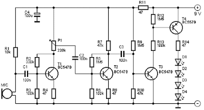
This is a Simple LED light Organ Circuit Diagram. This is a fun schema that can be at parties, for example. The four LEDs flash to the beat of the music. The light organ responds using a microphone to sound.T1 amplifies the signal from MIC. The sensitivity can be adjusted by P1. T4 controls the LEDs. 

These are preferably LEDs with a high light intensity.MIC is a condenser microphone. The schema can be powered by a 9 V battery.

 LED light Organ Circuit Diagram

 led light organ circuit diagram


The 4 Budget

This schema costs about € 6.15.


Parts List

  •      R1 = 10 k
  •      R2 = 330 K?
  •      R3, R6, R13 = 100 k
  •      R4, R8, R11, R14 = 47 Ω
  •      R5, R9, R12 = 1.5 MΩ
  •      R7, R10 = 47 k
  •      P1 = 220 K?
  •      C1, C2, C3 = 100 nF
  •      C4 = 100 uF
  •      D1-D4 = LED
  •      T1, T2, T3 = BC547B
  •      T4 = BC557B
  •      MIC = microphone capsule
Read More..

Monday, September 8, 2014

Simple Microprocessor power supply watchdog circuit Wiring diagram

The Simple Microprocessor power supply watchdog schema Diagram monitors the input to the microprocessor 5 V regulated supply for voltage drops and initiates a reset sequence before supply regulation is lost. In operation, the resistor capacitor combination Rs and Cj form a short time constant smoothing network for the output of the fullwave bridge rectifier. 

An approximately triangular, voltage waveform appears across C and Rs and it is the minimum excursion of this that initiates the reset. Diode Dg prevents charge sharing between capacitors Cj and Ck. Resistors Rn and Rm form a feedback network around the voltage reference section of the LM10C, setting a threshold voltage of 3.4 volts. 

 Microprocessor power supply watchdog schema Diagram

Simple


The threshold voltage is set at 90% of the minimum voltage of the triangular waveform. When the triangular wave trough, at the comparators non-inverting input, dips below the threshold, the comparator output is driven low. This presents a reset to the microprocessor. Capacitor Ch is charged slowly through resistor Rk and discharged rapidly through diode De.
Read More..

Thursday, September 4, 2014

Very simple FM Transmitter Bug


Most of viewers asked about FM transmitter schema today Im going to give you very small and some what powerful FM transmitter.The special thing of this schema is we can operate this schema with 3V.Here you can use BF414 / BF324 / BF606 transistor.


Read More..

Friday, August 29, 2014

Simple Panel Frequency Meter Wiring diagram Schematic

This is a Simple Panel Frequency Meter Circuit Diagram to measure the frequency of 230V AC mains. When you connect it to the 230V AC line, the display shows the line frequency. Generally, the line frequency is 50 Hz, which may vary from 48 Hz to 52 Hz. Beyond this frequency range, sensitive equipment may start malfunctioning.

The AC mains supply is stepped down by transformer X1 to deliver a secondary output of 9V-0-9V AC, 250 mA. The secondary output of the transformer is rectified by diodes D1 and D2, filtered by capacitor C1 and given to regulator IC1 to produce regulated 6V DC. 9V AC is also connected to pins 2 and 6 of IC2 via resistor R1. Timer IC2 converts the sinewave frequency sample of AC mains into a square wave that is more suitable for the schema operation.

Simple Panel Frequency Meter Circuit Diagram


Simple

Fig. 1: The schema of the panel frequency meter

IC CD4093 (IC3) is used as an oscillator-cum-divider. The oscillator, wired around gate N1, produces 10Hz clock. Decade counter IC4 divides 10Hz clock by 10 to produce 1Hz clock. The output of gate N1 is fed back to its inputs via potentiometer VR1 and resistor R4. Capacitor C2 connected between the inputs of gate N1 and ground charges/discharges depending on the logic level at the output of gate N1. The values of VR1, R4 and C2 are selected to produce accurate 10Hz clock.

Decade counter IC CD4017 (IC4) divides the output of IC3 by 10 to provide one pulse per second. LED1 connected to pin 12 of IC4 gives one flash per second to indicate that the oscillator and the counter are working properly.

Top
 Fig. 2: Top and bottom views of LTS543 common-cathode, 7-segment displays

This 1Hz clock is fed to clock pin 14 of decade counter IC CD4017 (IC5), whose Q0 output is given to pin 2 and the square wave produced by IC2 is given to pin 1 of AND gate N1. Therefore, the unknown frequency of AC mains line, applied to pin 1 of AND gate N1, passes through it for only one second and the number of clocks per second are counted by IC7 and IC8.

Decade counters/7-segment decoders IC7 and IC8 are cascaded to drive common-cathode, 7-segment displays DIS1 and DIS2 (each LTS543). DIS1 shows units place of the frequency and DIS2 shows tens place. The top and bottom views of LTS543 common-cathode, 7-segment displays are shown in Fig. 2.

This is an auto-reset schema. You can select the reset time of 1 second through 5 seconds using rotary switch S2, which is connected to reset pins of IC5, IC7 and IC8. For long-time display of the frequency, keep the knob of rotary switch S2 towards fifth position. Keeping rotary switch S2 to first position (minimum reset time) allows you to instantly see any variation in the supply frequency on the display. Also, while adjusting the generator frequency to mains frequency, keep rotary switch S2 towards first position.


Author:  V. David Sourced By: EFY
Read More..

Thursday, August 28, 2014

Simple Positive Regulator Wiring diagram Schematic

In the Simple Positive Regulator Circuit Diagram, Ql and Q2 are connected in the classic SCR or thyristor configuration. Where higher input voltages or minimum component count are required, the schema for thyristor boost can be used. 

  Positive Regulator Circuit Diagram

 positive regulator circuit diagram


The thyristor is running in a linear mode with its cathode as the control terminal and its gate as the output terminal. This is known as the remote base configuration.
Read More..

Tuesday, August 26, 2014

Simple Sound Operated Switch Wiring diagram Schematic

This is a Simple Sound Operated Switch Circuit Diagram. This sound-operated switch will sense the ring of the phone and translate this to a lamp that will go on and off. The amplified signal across R2 reaches D1 through capacitor C2. The rectified audio signals provide a negative bias for Q2, a pnp transistor. This causes Q2 to conduct so the current that triggers SCR1 is provided at the gate. Potentiometer R4 sets the sensitivity. R3 and C3 delay the operating voltage for Ql so that the schema will not be triggered on by the sound of the on/off switch, SI or by the current surge. Set the lamp atop a TV receiver, turn it on and set the potentiometer so that a finger snap at two feet will trigger the lamp on. Place the speaker close to the telephone and give it a try.

Simple Sound Operated Switch Circuit Diagram


Simple
Read More..

Sunday, August 24, 2014

Simple Switching Regulator Wiring diagram Schematic

This is the simple switching regulator schema diagram. The LTC10432 switched-capacitor building block provides nonoverlapping complementary drive to the Ql to Q4 power MOSFETs. The MOSFETs are arranged so that Cl and C2 are alternately placed in series and then parallel. During the series phase, the + 12 V battery`s current flows through both capacitors, charging them, and furnishing load current. 

During the parallel phase, both capacitors deliver current to the load. Ql and Q2 receive similar drive from pins 3 and 11. The diode-resistor networks provide additional nonoverlapping drive characteristics, preventing simultaneous drive to the series-parallel phase switches. Normally, the output would be one-half of the supply voltage, but C1 and its associated components close a feedback loop, forcing the output to 5 V. With the schema in the series phase, the output heads rapidly positive. 

When the output exceeds 5 V, Cl trips, forcing the LTC1043 oscillator pin, trace D, high; this truncates the LTC1043`s triangular-wave oscillator cycle. The schema is forced into the parallel phase and the output coasts down slowly, until the next LTC1043 clock cycle begins. Cl`s output diode prevents the triangle down-slope from being affected and the 100-pF capacitor provides sharp transitions. The loop regulates the output to 5 V by feedback controlling the turn-off point of the series phase.

Simple Switching Regulator Circuit Diagram


Read More..

Saturday, August 23, 2014

Simple 2 Door Annunciator Wiring diagram Schematic

Security system or alarms such as doorbell and Door Annunciator are most wanted in industries and institutional use. This is a Simple 2 Door Annunciator Circuit Diagram. When the push buttons at either door are depressed, this schema generates a different tone for each door. Tones are generated by phase-shift oscillator Q1/Q2. Q3 provides tone frequency change by changing the phase-shift network. U2 and U3 are timers for the tones and Q4/Q5 interface the timers with the push buttons. 

Simple 2 Door Annunciator Circuit Diagram


Read More..

Friday, August 22, 2014

Simple 6V lamp Flasher Wiring diagram Schematic


This is a simple lamp flasher schema diagram.Here you  can use 6V lamp.I have added this for my bike.oh it is great at night I have used blue color bulb.


Note 

# Dont supply over 6V for this schema 
# Build this schema on a PCB
Read More..

Thursday, August 21, 2014

Simple Portable Nicad Battery Charger Wiring diagram Schematic

This is a Simple Portable Nicad Battery Charger Circuit Diagram. This Simple Portable Nicad Battery Charger Circuit Diagram was designed to charge NiCad battery packs in the range of 4.8 to 15.6 V from a convenient remote power source, such as an automobile batter. 

 Portable Nicad Battery Charger Circuit Diagram


Portable

When power is first applied to the schema, a small bias current supplied by Rl via winding Wl, starts to turn on the transistor TRl. This forces a voltage across W2 and the positive feedback given by the coupling of Wl and W201uses the transistor to turn hard on, applying the full supply across W2. The base drive voltage induced across Wl makes the junction between Rl and R2 become negative with respect to the 0-V supply, forward-biasing diode Dl to provide the necessary base current to hold TRl on. 

With the transistor on, a magnetizing current builds up in W2, which eventually saturates the ferrite core of transformer Tl. This results in a sudden increase on the collector current flowing through TRl, causing its collector-emitter voltage to rise, and thus reducing the voltage across W2. 

The current flowing in W2 forces the collector voltage of the TRl to swing positive until restricted by transformer output loading. Rc network R4 and C3limits the turn off transient TRl. R3 and C2 maintain the loop gain of the schema when diode Dl is not conducting.
Read More..

Simple IR Remote Control Extender Wiring diagram Schematic

Description:
An Infra Red wired Repeater schema to control appliances from a remote location.

IR


Parts List:
R1: 1k Resistor (1)
R2: 3.3k Resistor (1)
R3: 10k Resistor (1)
R4: 15k Resistor (1)
R5: 2k2 Resistor (1)
R6: 470R Resistor (1)
R7: 47R Resistor (1) 0.5 Watt
PR1: 4.7k Preset (1)
C1,C3: 47u Elect(2)
C2: 1n Polyester 5% or better (1)
C4: 100u Elect(1)
Z1: 5V1 Zener (1)
Q1: BC549C or BC109C or 2N2222 (1)
Q2: BC337 or BC549 or ZTX450 (1)
IC1 : TSOP1738
IC2: 555 or 7555 (1)
LED1 5mm RED (1)
LED2,3 IR diode TIL38 or similar (2)

Alternatives to IC1 :

Everlight IR receiver module ELIRM 8621
Harrison electronics IR1
Vishay TSOP 1838
Radio Shack 276-0137
Sony SBX 1620-12
Sharp GP1U271R 

Notes:
The signal emitted by an IR remote control contains two parts, the control pulses and a modulated carrier wave. The control pulses are used to modulate the carrier, a popular modulation frequency being 36 and 42KHz. The signal is radiated by an IR diode, typical wavelengths in the 850 and 950 nm region of the electromagnetic spectrum. Although this light is invisible to the human eye, it can be seen as a bright spot with a camcorder or digital camera.

In this schema, the TSOP1738 IR module removes the carrier leaving only the slower control pulses ( 1 - 3KHz) which appear at the output. R1, C1 and Z1 form a smoothed 5 Volt supply for the IR module. Under quiescent conditions (no input signal) the output of the IR module is high. Transistor Q1 will be on, resulting in a low collector voltage, restting the 555 oscillator. Q1 also acts as a level shifter, converting the 5 Volt output signal to 12 Volts for the 555 timer. When an IR signal is received, decoded control pulses turn Q1 off and on. Each time Q1 turns off, pin 4 of the 555 timer goes high and an oscillation will be produced for the duration of each data pulse.

The 555 is wired as an equal mark/space ratio oscillator, the timing resistor R4, being connected back to the output of the timer, pin 3. The timing capacitor C2 is the other component in the timing chain. The pulse duration at pin 3 is defined as:-

T = 1.4 R4 C2

As the timing is crucialthe capacitor should have a tolerance of 5% or better and the power supply should be regulated. To allow for tolerance in components a 4k7 preset resistor is wired in series with R4. This adjustment allows R4 to be 15k to 19.7K creating output pulses of 21us and 27.58 us. As frequency is the reciprocal of periodic time then the oscillator adjustment is from 36.2Khz to 47KHz, allowing fine tuning for almost any appliance.

The final output stage uses a BC337 transistor in emitter follower. The output pulse will not be inverted, and the current through the IR photo emitters is around 30 mA dc. This is of course an average value, measured with a digital multimeter. The red led as always, is a visible indication that an input signal has been received. The schema may be modified to use a fixed resistor in the timing chain as shown below. In this example a voltage regulator is also recommended to prevent changes in supply voltage altering the output pulse.
IR

Setup and Testing:

Remove LED 2 and 3 and apply power. With no input signal LED 1 should be off. Press a button on a remote control in the same room as the schema. LED 1 should flicker. If all is well, connect LEDs 2 and 3 and point them in the direction of the appliance (TV or VCR etc). The cable to the LEDs can exceed 100 metres if necessary, ordinary loudspeaker cable or bell wire is suitable. Set preset PR1 midway initially, it should work for all equipment. Most equipment is tolerant to within 5% so if you have for example a video that works at 42kHz and a TV that works at 38Kz tuning the modulation to 40KHz should allow both devices to operate. Any troublesome equipment, for example an Echostar receiver repeatedly press abutton on the handset while tuning PR1, you will find that it operates at some point. One IR LED may be used in place of LED2 & 3, but if there are two appliance in the same room, but in different locations, LED 2 can be aimed at a video, while LED3 aimed at a CD player for example. Below is how I discretely placed a photo emitter and plastered it directly into the wall:
IR

Modifications:

An alternative output configuration is shown below. This uses a MOSFET to replace the original BC337 transistor. My thanks to Pete Griffiths for this modification and diagram.
IR

Compatability:

If you make either the Mark 3 or 4 schema please let me know if it works and the make and model of your remote control. I will add this to the database of compatible handsets below:-  link

Aiwa RC-ZVR01
Denon RC 554
Denon RC 921
Denon RC 924
Echostar T22605AA-00 * troublesome required careful tuning of PR1 to work
Kameleon One for all remote (URC-8060) Goodmans 97P1R2CPA1
Grundig SRC2
JVC LP20878-002
Matsui 28WN04
Mitsubishi 290P103A10
Mitsubishi EUR647003
NAD HTR2 (multi remote)
One for All 9910
Panasonic EUR511200
Philips RC6512
Pioneer AXD7323
Pioneer DV444
Pioneer VXX2801
Radioshack 1995
Saisho VR3300X
Sony RM-533
Sony RM-887
Sony RMT-V240
Sony RM-S325
Sony RM-DX50
Sony RM-U215
Sony RM-839
Sony RM-SCEX1
Sony RM-S336
Sony RM-D43M
Sony VCR
Technics EUR64713
Read More..