Showing posts with label diagram. Show all posts

Friday, December 12, 2014

Broadcast Transmitter Circuit Diagram

transmitter-schematic


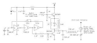
In this circuit, a 74HC14 hex Schmitt trigger inverter is used as a square wave oscillator to drive a small signal transistor in a class C amplifier configuration.The oscillator frequency can be either fixed by a crystal or made adjustable (VFO) with a capacitor/resistor combination.
Read More..

Thursday, November 13, 2014

Borg Warner Truck Wiring Diagram

The following truck wiring diagram is originally scanned from 1965 Chilton’s manual. Should you have an all original truck with overdrive, this diagram should be usable. This manual contains a diagram for wiring a split control setup for your T-85N transmission. This can be used for one you’ve bought outright and have no original circuit for, or modifying the one you already have. The DPDT relay is Double Pole Double Throw relay.

Find more detail information about Borg Warner Truck Wiring Diagram in the following article. (source: hydratech.com)

Read More..

Thursday, October 16, 2014

Motorcycle Alarm With Transistor Circuit Diagram

This is a simple Motorcycle Alarm With Transistor Circuit Diagram. Its designed to work at 12-volts. But - if you change the relay for one with a 6-volt coil - itll protect your "Classic Bike". The standby current is virtually zero - so it wont drain your battery.

Motorcycle Alarm With Transistor Circuit Diagram

Motorcycle

Any number of normally-open switches may be used. Fit the mercury switches so that they close when the steering is moved or when the bike is lifted off its side-stand or pushed forward off its centre-stand. Use micro-switches to protect removable panels and the lids of panniers etc. While at least one switch remains closed - the siren will sound.

About one minute after all of the switches have been opened again - the alarm will reset. How long it takes to switch off depends on the characteristics of the actual parts youve used. You can adjust the time to suit your requirements by changing the value of C1 and/or R3.

The circuit is designed to use an electronic Siren drawing 300 to 400mA. Its not usually a good idea to use the bikes own Horn because it can be easily located and disconnected. However, if you choose to use the Horn, remember that the alarm relay is too small to carry the necessary current. Connect the coil of a suitably rated relay to the Siren output - and use its contacts to sound the horn.

The circuit board and switches must be protected from the elements. Dampness or condensation will cause malfunction. Without its terminal blocks, the board is small. Ideally, you should try to find a siren with enough spare space inside to accommodate it. Fit a 1-amp in-line fuse as close as possible to the power source. This is Very Important. The fuse is there to protect the wiring - not the circuit board. Instead of using a key-switch you can use a hidden switch; or you could use the normally-closed contacts of a small relay. Wire the relay coil so that its energized while the ignition is on. Then every time you turn the ignition off - the alarm will set itself.

When its not sounding, the circuit uses virtually no current. This should make it useful in other circumstances. For example, powered by dry batteries and with the relay and siren voltages to suit, it could be fitted inside a computer or anything else thats in danger of being picked up and carried away. The low standby current and automatic reset means that for this sort of application an external on/off switch may not be necessary.

When you set the alarm - if one of the switches is closed - the siren will sound. This could cause annoyance late at night. A small modification will allow you to Monitor The State Of The Switches using LEDs. When the LEDs are all off - the switches are all open - and its safe to turn the alarm on.

Veroboard Layout

Veroboard


Read More..

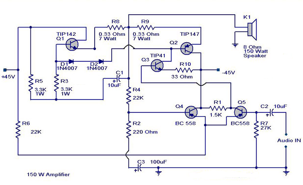
Simple 150W Amplifier Circuit Diagram

This is the cheapest 150 Watt amplifier circuit you can make,I think.Based on two Darlington power transistors TIP 142 and TIP 147 ,this circuit can deliver a blasting 150 W Rms to a 4 Ohm speaker.Enough for you to get rocked?;then try out this.

TIP 147 and 142 are complementary Darlington pair transistors which can handle 5 A current and 100V ,famous for their ruggedness. Here two BC 558 transistors Q5 and Q4 are wired as pre amplifier and TIP 142 ,TIP 147 together with TIP41  (Q1,Q2,Q3) is used for driving the speaker.This circuit is designed so rugged that this can be assembled even on a perf board or even by pin to pin soldering.The circuit can be powered from a +/-45V, 5A  dual power supply.You must try this circuit.Its working great!

The preamplifier section of this circuit is based around Q4 and Q5 which forms a differential amplifier. The use of a differential amplifier in the input stage reduces noise and also provides a means for applying negative feedback. Thus overall performance of the amplifier is improved. Input signal is applied to the base of Q5 through the DC decoupling capacitor C2. Feedback voltage is applied to the base of Q4 from the junction of 0.33 ohm resistors through the 22K resistor. A complementary Class AB push-pull stage is built around the transistors Q1 and Q2 for driving the loud speaker. Diodes D1 and D2 biases the complementary pair and ensures Class AB operation. Transistor Q3 drives the push-pull pair and its base is directly coupled to the collector of Q5.

 150W Amplifier Circuit Diagram

 150w amplifier circuit diagram

Notes.

  • Remember TIP 142 and 147 are Darlington pairs  .They are shown as conventional transistors in figure for ease.So don’t get confused.Even though each of them have 2 transistors ,2 resistors and 1 diode inside ,only three pins ,base emitter and collector are coming out.Rest are connected internally.So its quite OK to assume each of them as transistor for ease.
  • Use a well regulated and filtered power supply.
  • Connect a 10K POT in series with the input as volume control if you need.Not shown in circuit diagram.
  • All electrolytic capacitors must be rated at least 50volts.

Power supply for this circuit.

A  +40/-40 unregulated dual supply for powering this amplifier project is shown below.  This power supply is only enough for powering one channel and for stereo applications double the current ratings of  the transformer, diodes and fuses.


Read More..

Wednesday, October 15, 2014

Burglar Alarm With Timed Shutoff Circuit Diagram

When SI (sensor) is closed, power is applied to U2, a dual timer. After a time determined by C2, CI is energized after a predetermined time determined by the value of C5, pin 9 of U2 becomes low, switching off the transistor in the optoisolater, cutting anode current of SCR1 and de-energizing Kl. The system is now reset. Notice that (i6x C2) is less than (R7xC$). The ON time is approximately given by:(R7xC5)-(R6xC2) = Ton 


Burglar Alarm With Timed Shutoff Circuit Diagram


Read More..

Phase Controlled Dimmer Circuit Diagram

A phase-controlled dimmer delays the triac turn-on to a selected point in each successive ac half cycle. Use this circuit only for incandescent lamps, heaters, soldering irons, or universal motors that have brushes.

Phase Controlled Dimmer Circuit Diagram


Phase

Read More..

Monday, October 13, 2014

Volvo 700 B230K Engine Ignition System Wiring Diagram

During the production between 1982–1990, the Volvo 700 series (760, 740, 780) were available in many different engine types and capacities, among others are 2.3 L B23ET 173 hp (129 kW) turbo I4; 2.3 L B230FT 156/165 hp turbo I4; 2.8 L B280F 147 hp V6 and 2.4 L D24TIC 115 hp (86 kW) turbo diesel I6. Below schematic depicts the 1982 Volvo Volvo 700 B230K Engine Ignition System Wiring Diagram.

Volvo

1. Battery
2. Ignition Switch
4. Ignition Coil
5. Distributor
6. Spark Plugs
11. Fuse box
29. Positive Terminal Board
81. AC Pressure Switch
86. Rev Counter
156. Radiator Fan Motor
200. AC Compressor Solenoid
202. Climate Control
218. Knock Sensor
224. Radiator Fan Thermostat
260. Control Unit
267. Test Connector
271. Fuel Cut-off Solenoid
272. Micro switch
273. Temperature Sensor
293. Idling Compensation relay
419. Power Stage
A. Connector, RH A-Post
B. Connector, LH A-Post
C. Connector, at LH Wheel Housing
D. Ground Terminal on Intake Manifold
E. Connector at LH Wheel Housing
Read More..

Power Monitor Circuit Diagram

Here is a simple non-contact AC power monitor for home appliances and laboratory equipment that should remain continuously switched-on. A fuse failure or power breakdown in the equipment going unnoticed may cause irreparable loss. The monitor sounds an alarm on detecting power failure to the equipment. The circuit is built around CMOS IC CD4011 utilising only a few components. NAND gates N1 and N2 of the IC are wired as an oscillator that drives a piezobuzzer directly. Resistors R2 and R3 and capacitor C2 are the oscillator components. The amplifier comprising transistors T1 and T2 disables the oscillator when mains power is available. In the standby mode, the base of T1 picks up 50Hz mains hum during the positive half cycles of AC and T1 conducts.

Non-Contact Power Monitor Circuit diagram:
   
Non-Contact Power Monitor circuit diagram
  
This provides base current to T2 and it also conducts, pulling the collector to ground potential. As the collectors of T1 and T2 are connected to pin 2 of NAND gate N1 of the oscillator, the oscillator gets disabled when the transistors conduct. Capacitor C1 prevents rise of the collector voltage of T2 again during the negative half cycles. When the power fails, the electrical field around the equipment’s wiring ceases and T1 and T2 turn off. Capacitor C1 starts charging via R1 and preset VR and when it gets sufficiently charged, the oscillator is enabled and the piezobuzzer produces a shrill tone. Resistor R1 protects T2 from short circuit if VR is adjusted to zero resistance.

The circuit can be easily assembled on a perforated/breadboard. Use a small plastic case to enclose the circuit and a telescopic antenna as aerial. A 9V battery can be used to power the circuit. Since the circuit draws only a few microamperes current in the standby mode, the battery will last several months. After assembling the circuit, take the aerial near the mains cable and adjust VR until the alarm stops to indicate the standby mode. The circuit can be placed on the equipment to be monitored close to the mains cable.
Read More..

Thursday, October 2, 2014

Circuit Diagram FM Antenna Booster

FM
FM Antenna Booster Circuit Diagram

This is a low cost fm antenna booster that can be used to listen to programmes from distant FM stations clearly. The antenna fm booster circuit comprises a common-emitter tuned RF preamplifier wired around VHF/UHF transistor 2SC2570 (C2570).

Assemble the circuit on a good-quality PCB (preferably, glass-epoxy). Adjust input/output trimmers (VC1/VC2) for maximum gain.

Input coil L1 consists of four turns of 20SWG enamelled copper wire (slightly space wound) over 5mm diameter former. It is tapped at the first turn from ground lead side. Coil L2 is similar to L1, but has only three turns. Pin configuration of transistor 2SC2570 is shown in the fm antenna booster schematic.
Read More..

Thursday, September 25, 2014

Accurate Capacitance Meter Circuit Diagram

  1. The charges on Cr and CX are now equal and the meter indicates by how much the voltage across CX differs from that across Cy. Buffer IC3 presents a very high load impedance to CX.
  1. This relies on the formula C = O/V where C is the capacitance in Farads, O is the charge in Coulombs and V is the voltage in volts. lf therefore two capacitances have equal charges, their values can be calculated when the voltages across them are known.
  2. Each time the output of gate N2 rises, the charges of capacitors C2 and C3 are transferred to Cr and CX by trensistors Tl and T3 respectively.
  3. For instance, to enable a capacitor of 470 pF to be measured, C2 and C3 have to be 10. . . 20 pF.
  4. The circuit is reasonably accurate for values of CX up to 100 uF:
  5. Two circuits ensure that reference capacitor Cr and the capacitor to be measured, CX, are charged equally. The circuit for Cr consists of C2, D1 and T1 and that for CX of C3, D2 and T3.
  6. ln this capacitance meter, the value of a capacitor is determined by giving it the same charge as a refer- ence capacitance and then comparing the voltages across them.
  7. The voltage across Cr is compared by lC2 with a reference voltage derived from the power supply via R3/R4. When the voltage across Cr ‘ exceeds the reference voltage, com- parator IC2 inverts which inhibits N2 and causes N3 to light LED D3.
  8. When the output of N2 drops, C2 and C3 recharge via diodes D1 and D2. Gate N2 is controlled by astable multivibrator N 1 which operates at a frequency of about 2 kl-lz: Cr and CX are therefore charged at that frequency.
  9. Above that value the y measurement will be affected by leakage currents. To measure capacitors of up to 100 pF, the values of C2 and C3 should be increased to 1 AF. c l Current consumption is minimal so that a 9 V battery is an adequate power supply.
  10. Pressing reset button S1 causes both Cr and CX to discharge via T2 and T4 respectively, after which the charging process restarts and the circuit is ready for the next measurement. The meter is calibrated by using two identical 10 nF capacitors for Cr and CX. Press the reset button and, when the LED lights, adjust preset P1 to give a meter reading of exactly one tenth of full scale deflection (fsd). That reading corresponds to 1 x Cr.
  11. lf, therefore, Cr = 100 nF and CX = 470 nF, the meter will read 0.47 of fsd. To ensure a sufficient number of charging cycles during a measure· ment, Cr and CX-should not be smaller than 4.7nF. To measure l smaller values, capacitors C2 and C3 will have to be reduced. 

Read More..

Monday, September 22, 2014

Automotive 12V to 20V converter for audio amplifier descriptiona and circuit diagram

Circuit diagrams

The limitation of car supply voltage (12V) forces to convert the voltages to higher in order to power audio amplifiers.
In fact the max audio power x speaker (with 4 ohm impedance) using 12V is (Vsupply+ - Vsupply-)^2/(8*impedance) 12^2/32 = 4.5Watts per channel, that is laughable...
For powering correctly an amplifier the best is to use a symmetric supply with a high voltage differential. for example +20 - -20 = 40Volts
in fact
40^2/32 = 50 Watts per channel that is respectable.
This supply is intended for two channels with 50W max each (of course it depends on the amplifier used). Though it can be easily scaled up or the voltages changed to obtain different values.

Overview - How it works
It is a classic push-pull design , taking care to obtain best symmetry (to avoid flux walking). Keep in mind that this circuit will adsorb many amperes (around 10A) so take care to reinforce power tracks with lots of solder and use heavy wires from the battery or the voltage will drop too much at the input.
The transformer must be designed to reduce skin effect, it can be done using several insulated magnet wire single wires soldered together but conducting separately. The regulation is done both by the transformer turn ratio and varying the duty cycle. In my case i used 5+5 , 10+10 turns obtaining a step up ratio of 2 (12->24) and downregulating the voltage to 20 via duty cycle dynamic adjust performed by the PWM controller TL494.
The step-up ratio has to be a little higher to overcome diode losses, winding resistance and so on and input voltage drop due to wire resistance from battery to converter.

Transformer design
The transformer must be of correct size in order to carry the power needed, on the net there are many charts showing the power in function of frequency and core size for a given topology. My transformer size is 33.5 mm lenght, 30.0 height and 13mm width with a cross section area of 1,25cm^2, good for powers around 150W at 50khz.
The windings , especially the primary must be heavy gauged, but instead of using a single wire it is better to use
multiple wires in parallel each insulated from the other except at the ends. This will reduce resistance increase due to skin effect. The primary and secondary windings are centertapped, this means that you have to wind 5 turns, centertap and 5 windings again. The same goes for the secondary, 10 turns, centertap and 10 turns again.
The important thing is that the transformer MUST not have air gaps or the leakage inductance will throw spikes on the switches overheating them and giving a voltage higher than expected by turn ratio prediction, so if your voltage output (at fully duty cycle) is higher than Vin*N2/N1 - Vdrop diode, your transformer has gap (of course permit me saying you that you are BLIND if you miss it), and this is accompanied with a drastical efficiency reduction. Use non-gapped E cores or toroids (ferrite).

Output diodes, capacitors and filter inductor
For rectification i preferred to use shottky diodes since they have low forward voltage drop, and are incredibly fast.
I used the cheap 1N5822, the best alternative for low voltage converters (3A for current capability).
The output capacitors are 4700uF 25V, not very big, since at high frequency the voltage ripple is most due to internal cap ESR fortunately general purpose lytics have enough low esr for a small ripple (some tens of millivolts). Also at high duty cycle they are feed almost with pure DC, giving small ripple. The filter inductor on the secondary centertap furter increases the ripple and helps the regulation in asymmetrical transients

Power switch and driving
I used d2pak 70V 80A 0.004 ohms ultrafets (Fairchind semiconductor), very expensive and hard to find. In principle any fet will work, but the lower the on-resistance, the lower the on-state conduction losses, the lower the heat produced on the fets, the higher efficiency and smaller the heatsinks needed. With this fets i am able to run the fets with small heatsinks and without fan at full rated power (100W) with an efficiency of 82% and perceptible heating and with small heating at 120W (some degrees) (the core starts to saturate and the efficiency is a bit lower, around 75%)
Try to use the lowest resistance mosfet you can put your dirty hand :-) on or the efficiency will be lower than rated and you will need even a small fan. The fet driver i used is the TPS2811P, from Texas instruments, rated for 2A peak and 200ns. Is important that the gate drive is optimized for minimal inductance or the switching losses will be higher and you risk noise coupling from other sources. Personally i think that twisted pair wires (gate and ground/source) are the best to keep the inductance small. Place the gate drive resistor near the Mosfet, not near the IC.

Controller
I used the trusty TL494 PWM controller with frequency set at around 40-60 Khz adjustable with a potentiometer. I also implemented the soft start (to reduce powerup transients). The adjust potentiometer (feedback) must be set to obtain the desired voltage. The output signals is designed with two pull-up resistors on the collector of the PWM chip output transistor pulling them to ground each cycle alternatively. This signal is sent to the dual inverting MOSFET driver (TPS2811P) obtaining the correct waveform.

Power and filtering
How i said before the power tracks must be heavy gauged or you will scarify regulation (since it depends of transformer step up ratio and input voltage) and efficiency too. Dont forget to place a 10A (or 15A) fuse on the input because the car batteries can supply very high currents in case of shorts and this will save you face from a mosfet explosion in case of failture or short, remember to place a fuse also on the battery side to increase the safety (accidental shorts->fire, battery explosion, firemen, police and lawyers around). Input filtering is important, use at least 20000uF 16V in capacitors, a filter inductor would be useful too (heavygauged) but i decided to leave it..

Final considerations
This supply given me up to 85% efficiency (sometimes even 90% at some loads) with an input of 12V because i observed all these tricks to keep it functional and efficient. An o-scope would be useful, to watch the ripple and gate signals (watching for overshoots), but if you follow these guidelines you will avoid these problems.
The cross regulation is good but keep in mind that only the positive output is fully regulated, and the negative only follows it. Place a small load between the negative rail and ground (a 3mm led with a 4.7Kohm resistor) to avoid the negative rail getting lower then -20V. If the load is asymmetric you can have two cases:
-More load on positive rail-> no problems, the negative rail can go lower than -20V, but it is not a real issue for an audio amplifier.
-More load on negative rail-> voltage drop on negative rail (to ground) especially if the load is only on the negative rail.
Fortunately audio amplifiers are quite symmetrical as a load, and the output filter inductor/capacitors helps to maintain the regulation good during asymmetrical transients (Basses)

FOR FIRST TESTING USE A SMALL 12V power supply and use resistors as load monitoring switches heat and current consumption (and output) and try to determine efficiency, if it is higher then 70-75% you are set, it is enough. Adjust the frequency for best compromise between power and switching losses, skin effect and hysteresis losses

Bill Of Materials
=================
Design: 12V to 20V 100W DC-DC conv
Doc. no.: 1
Revision: 3
Author: Jonathan Filippi
Created: 29/04/05
Modified: 18/05/05

Parts
2 R1,R2 = 10
4 R3,R4,R6,R7 = 1k
1 R5 = 22k
1 R8 = 4.7k
1 R9 = 100k
2 C1,C2 = 10000uF
2 C3,C6 = 47u
1 C4 = 10u
3 C5,C7,C14 = 100n
2 C8,C9 = 4700u
1 C12 = 1n
1 C13 = 2.2u
1 U1 = TL494
1 U2 = TPS2811P
2 Q1,Q2 = FDB045AN
4 D1-D4 = 1N5822
1 D5 = 1N4148
1 FU1 = 10A
1 L1 = 10u
1 L2 = FERRITE BEAD
1 RV1 = 2.2k
1 RV2 = 24k
1 T1 = TRAN-3P3S


author: Jonathan Filippi
e-mail: jonathan.filippi@virgilio.it
web site: http://www.cool-science.tk
Read More..

Sunday, September 21, 2014

12VDC Fluorescent Lamp Driver circuit diagram and description

A number of people have been unable to find the transformer needed for the Black Light project, so I looked around to see if I could find a fluorescent lamp driver that does not require any special components. I finally found one in Electronics Now. Here it is. It uses a normal 120 to 6V stepdown transformer in reverse to step 12V to about 350V to drive a lamp without the need to warm the filaments.

Circuit diagram

Parts:
C1 100uf 25V Electrolytic Capacitor
C2,C3 0.01uf 25V Ceramic Disc Capacitor
C4 0.01uf 1KV Ceramic Disc Capacitor
R1 1K 1/4W Resistor
R2 2.7K 1/4W Resistor
Q1 IRF510 MOSFET
U1 TLC555 Timer IC
T1 6V 300mA Transformer
LAMP 4W Fluorescent Lamp
MISC Board, Wire, Heatsink For Q1

Notes:
1. Q1 must be installed on a heat sink.
2. A 240V to 10V transformer will work better then the one in the parts list. The problem is that they are hard to find.
3. This circuit can give a nasty (but not too dangerous) shock. Be careful around the output leads. 

Read More..

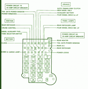
Explanation Fuse Box Chevrolet Suburban 89 Diagram

Fuse Box Chevrolet Suburban 89 Diagram - This show you about Fuse Box Chevrolet Suburban 89 Diagram.

Fuse Box Chevrolet Suburban 89 Diagram


Fuse
Fuse

Fuse Panel Layout Diagram Parts: tailgate, power window, rear defogger, cruise control, diesel auxiliary fuel, tank selector switch, clock, cargo lamp, auto trans, auxiliary battery, rear defogger, rear heater, power locks.
Read More..

Saturday, September 20, 2014

Mercedes Explanation Fuse Box Year Benz 1997 1998 F150 Diagram

Fuse Box Mercedes Benz 1997 & 1998 F150 Diagram - Below is Fuse Box Mercedes Benz 1997 & 1998 F150 Diagram.

Fuse Box Mercedes Benz 1997 & 1998 F150 Diagram


Fuse
Fuse

Fuse Panel Layout Diagram Parts: powetrain control module, trailer tow stop/turn lamps.
Read More..

Friday, September 19, 2014

Mercedes Explanation Fuse Box Year Benz 1990 300 Diagram

Fuse Box Mercedes Benz 1990 300 Diagram - Below is Fuse Box Mercedes Benz 1990 300 Diagram.

Fuse Box Mercedes Benz 1990 300 Diagram


Fuse
Fuse

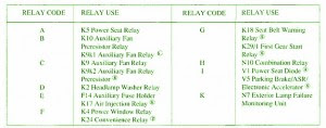
Fuse Panel Layout Diagram Parts: power seat relay, auxiliary fan, resistor relay, headlamp, washer, air injection, power window, convenience relay, seat belt warning relay, gear start relay, combination relay, power seat diode, parking brake, exterior lamp.
Read More..

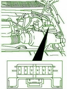
Fuse Box Ford 1999 Ranger XLT 2 5 lit Diagram

Fuse Box Ford 1999 Ranger XLT 2.5 lit Diagram - Here are new post for Fuse Box Ford 1999 Ranger XLT 2.5 lit Diagram.

Fuse Box Ford 1999 Ranger XLT 2.5 lit Diagram


Fuse
Fuse

Fuse Panel Layout Diagram Parts: PCM power, horn, parking lamp, headlamp, PCM, low fluid resistor, RABS diode, PCM power diode, power window, ignition, I/P fuse panel, blower motor, ABS pump, A/C clutch system, 4wheel drive, fog lamp, ABS module.
Read More..

Wednesday, September 17, 2014

Fuse Box BMW E36 Diagram

Fuse Box BMW E36 Diagram - Here are new post for Fuse Box BMW E36 Diagram.

Fuse Box BMW E36 Diagram


Fuse
Fuse

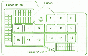
Fuse Panel Layout Diagram Parts: Taillight/Foglight Relay, System (main) Relay, Fuel Pump Relay, Oxygen Sensor Heater Relay, Emergency Flasher Relay, Horn Relay, High Beam Relay.
Read More..

Fuse Box Ford 66 Montego Diagram

Fuse Box Ford 66 Montego Diagram - Here are new post for Fuse Box Ford 66 Montego Diagram.

Fuse Box Ford 66 Montego Diagram


Fuse
Fuse

Fuse Panel Layout Diagram Parts: terminal, fuse emergency flasher, cigar lighter, clock feed, fuse panel, fuse courtesy, dome, cargo, luggage, glove compartment lamp, instrument panel, cluster lamps, .fuse heater, warning lamps, seat belt warning, brake warning, brake warning, air conditioning, windshield washer, accessory feed.
Read More..

Tuesday, September 16, 2014

Fuse Box Ford 2010 Fusion Power Distribution Diagram

Fuse Box Ford 2010 Fusion Power Distribution Diagram - Here are new post for Fuse Box Ford 2010 Fusion Power Distribution Diagram.

Fuse Box Ford 2010 Fusion Power Distribution Diagram


Fuse
Fuse

Fuse Panel Layout Diagram Parts: power assist steering, powertrain control module, starter motor relay, anti lock brake system, wiper washer, ABS valve, transmission module, alternator, console power point, A/C clutch, cooling fan motor, fuel relay, passenger power point, driver power seat, fuel pump, one touch start, heated side mirrors, back up lamp, A/C clutch, Injector, generator powertrain component, ignition coil, blower motor relay, fuel relay, starter relay,PCM relay.
Read More..

Monday, September 15, 2014

Explanation Fuse Box Chevrolet Tracker 2001 Diagram

Fuse Box Chevrolet Tracker 2001 Diagram - This show you about Fuse Box Chevrolet Tracker 2001 Diagram.

Fuse Box Chevrolet Tracker 2001 Diagram


Fuse
Fuse

Fuse Panel Layout Diagram Parts: accessory power ooutlet, electronic fuel injecion system, headlamp, high beam indicator, heater, hazard lamp, rear combination lamp, dome light, horn, cigar lighter, radio, ignition coil, meter, wiper, washer, rear defroster, turn signal, back up lamp, anti lock brake system, all electrical loads, air conditioning.
Read More..