Monday, January 26, 2015
Low Cost Guitar Amplifier
The present circuit can deliver 10W of output power when driving an 8 Ohm load, or about 18W @ 4 Ohm. It also features a two-FET preamplifier, two inputs with different sensitivity, a treble-cut control and an optional switch allowing overdrive or powerful treble-enhancement.
P1______________4K7 Linear Potentiometer
P2_____________10K Log. Potentiometer
R1,R2__________68K 1/4W Resistors
R3____________220K 1/4W Resistor
R4,R6,R11_______4K7 1/4W Resistors
R5_____________27K 1/4W Resistor
R7______________1K 1/4W Resistor
R8______________3K3 1/2W Resistor
R9______________2K 1/2W Trimmer Cermet
R10___________470R 1/4W Resistor
R12_____________1K5 1/4W Resistor
R13___________470K 1/4W Resistor
R14____________33K 1/4W Resistor
C1____________100pF 63V Ceramic Capacitor
C2____________100nF 63V Polyester Capacitor
C3____________470µF 35V Electrolytic Capacitor
C4____________220nF 63V Polyester Capacitor (Optional, see Notes)
C5_____________47µF 25V Electrolytic Capacitor (Optional, see Notes)
C6______________1µF 63V Polyester Capacitor
C7,C8,C9,C10___47µF 25V Electrolytic Capacitors
C11____________47pF 63V Ceramic Capacitor
C12__________1000µF 35V Electrolytic Capacitor
C13__________2200µF 35V Electrolytic Capacitor
D1_____________5mm. Red LED
D2,D3________1N4004 400V 1A Diodes
Q1,Q2________2N3819 General-purpose N-Channel FETs
Q3____________BC182 50V 200mA NPN Transistor
Q4____________BD135 45V 1.5A NPN Transistor (See Notes)
Q5____________BDX53A 60V 8A NPN Darlington Transistor
Q6____________BDX54A 60V 8A PNP Darlington Transistor
J1,J2________6.3mm. Mono Jack sockets
SW1____________1 pole 3 ways rotary switch (Optional, see Notes)
SW2____________SPST Mains switch
F1_____________1.6A Fuse with socket
T1_____________220V Primary, 48V Center-tapped Secondary 20 to 30VA Mains transformer
PL1____________Male Mains plug
SPKR___________One or more speakers wired in series or in parallel, Total resulting impedance: 8 or 4 Ohm, Minimum power handling: 20W
Notes:
- SW1 and related capacitors C4 & C5 are optional.
- When SW1 slider is connected to C5 the overdrive feature is enabled.
- When SW1 slider is connected to C4 the treble-enhancer is enabled.
- C4 value can be varied from 100nF to 470nF to suit your treble-enhancement preferences.
- In all cases where Darlington transistors are used as the output devices it is essential that the sensing transistor (Q4) should be in as close thermal contact with the output transistors as possible. Therefore a TO126-case transistor type was chosen for easy bolting on the heatsink, very close to the output pair.
- To set quiescent current, remove temporarily the Fuse F1 and insert the probes of an Avo-meter in the two leads of the fuse holder.
- Set the volume control to the minimum and Trimmer R9 to its minimum resistance.
- Power-on the circuit and adjust R9 to read a current drawing of about 25 to 30mA.
- Wait about 15 minutes, watch if the current is varying and readjust if necessary.
Sensitivity:
30mV input for 10W output
Frequency response:
40 to 20KHz -1dB
Total harmonic distortion @ 1KHz and 10KHz, 8 Ohm load:
below 0.05% @ 1W, 0.08% @ 3.5W, 0.15% at the onset of clipping (about 10W).

Thursday, November 20, 2014
20W Car Audio Amplifier with LM1875
The IC is aswell arranged with a lot acceptable appearance like fast bulk rate, advanced accumulation voltage range, top achievement current, top achievement voltage swing, thermal aegis etc. The IC is accessible in TO-220 artificial ability amalgamation and is able-bodied acceptable for a array of applications like audio systems, servo amplifiers, home theatre systems etc.
Notes.
- Assemble the circuit on a good quality PCB.
- Use +/-25V DC dual supply for powering the circuit.
- K1 can be 4 ohm, 20W speaker.
- A proper heat sink is necessary for the IC.
- F1 and F2 are 2A
Wednesday, November 19, 2014
1000Watt Audio Power Amplifier Blazer Circuit
The transistors are 2SC3858 (NPN) and 2SA1494 (PNP), and have high bandwidth, wonderful safe operating space, high linearity and high gain. Driver transistors are 2SC5200 (NPN) and 2SA1943 (PNP). All devices are rated at 230V, with the facility transistors having a 150W dissipation and also the drivers are 50W.
This circuit describes an amplifier, power offer and tests procedures that are all inherently dangerous. Nothing described during this article ought to even be thought-about unless youre totally experienced, grasp specifically what youre doing, and are willing to require full 100% responsibility for what you are doing. There are aspects of the look which will need analysis, fault-finding and/or modification.
Monday, November 17, 2014
High Power Audio Amplifier 2800W
| Click schematic to view larger |
R2_____100Ω
R3_____2K2Ω
R4_____560Ω
R5_____1Ω
R6_____27KΩ
R7_____10KΩ
R8_____100Ω
R9_____100Ω
R10____100Ω
R11____12KΩ
R12____100Ω
R13____100Ω
R14____100Ω
R15____27KΩ
R16____2K2Ω
R17____560Ω
R18____100Ω
R19____10KΩ
R20____330Ω
R21____47Ω 2W
R22____56Ω
R23____2K2Ω
R24____22Ω
R25____56Ω
R26____180Ω
R27____500-1KΩ Trim
R28____560Ω
R29____56Ω
R30____56Ω
R31____22Ω 1W
R32____5Ω6 2W
R33____10Ω
R34____180Ω
R35____100Ω
R36____22Ω 2W
R37____180Ω
R38____56Ω
R39____47Ω 2W
R40____5Ω6 2W
R41____10Ω
R42____10Ω
R43____10Ω
R45____10Ω
R46____0.22Ω 5W
R47____0.22Ω 5W
R48____0.22Ω 5W
R49____0.22Ω 5W
R50____10Ω 5W
C2_____1.5nF
C3_____0.1цF 250-275V
C4_____0.1цF 250-275VC5_____100nF
C6_____100цF 50V
C7_____39pF
C8_____330pF
C9_____330pF
C10____330pF
C11____47nF 250-275V
C12____220nF 250-275V
T2_____2N5551 / C2240
T3_____2N5551 / C2240
T4_____2N5551 / C2240
T5_____2N5551 / C2240
T6_____2N5401 / BF423
T7_____2N5401 / BF423
T8_____2N5401 / BF423
T9_____2N5401 / BF423
T10____MJE350
T11____B1186
T12____TIP127
T13____D1763
T14____D1763
T15____B1186
T16____C5198
T17____A1941
T18____2SC2922 / MJ15024G
T19____2SC2922 / MJ15024G
T20____2SA1216 / MJ15025G
T21____2SA1216 / MJ15025G
| This installation include gain JRC4558 |
| This is pcb design |
| Installation with booster |
Sunday, November 16, 2014
TDA2006 12W Audio Amplifier Circuit
The TDA2006 is monolithic integrated circuit in package, {supposed to be used as a low frequency category "AB" amplifier. At ±12V, d = 10 and frequently it provides 12W output power on a 4Ω load and 8W on a 8Ω . The TDA2006 provides high output current and has terribly low harmonic and cross-over distortion. any the device incorporates an inspired (and patented) short circuit protection system comprising a rendezvous for automatically limiting the dissipated power therefore on keep the operating urpose of the output transistors at intervals their safe operating space. a standard thermal shutdown system is additionally included. The TDA2006 is pin to pin equivalent to the TDA2030
Saturday, November 15, 2014
2×5 W STEREO POWER AMPLIFIER CIRCUIT BASED ON BA5417
BA5417 Stereo Power Amplifier
Description
Circuit Diagram

Notes
- Supply voltage range of BA5417 is from 6 to 15V DC.
- The recommended supply voltage for this circuit is 12V DC.
- The power supply must be well regulated and filtered.
- BA5417 requires a heatsink.
- The circuit can be assembled on a perf board without much degradation in performance.
Saturday, November 8, 2014
LM1875 – POWER AMPLIFIER 20 WATT

The LM1875 delivers 20 watts into a 4Ω or 8Ω load on ±25V supplies. Using an 8 load and ±30V supplies, over 30 watts of power may be delivered. The amplifier is designed to operate with a minimum of external components. Device overload protection consists of both internal current limit and thermal shutdown.
The LM1875 design takes advantage of advanced circuit techniques and processing to achieve extremely low distortion levels even at high output power levels. Other outstanding features include high gain, fast slew rate and a wide power bandwidth, large output voltage swing, high current capability, and a very wide supply range. The amplifier is internally compensated and stable for gains of 10 or greater.
Features
• Up to 30 watts output power
• AVO typically 90 dB
• Low distortion: 0.015%, 1 kHz, 20 W
• Wide power bandwidth: 70 kHz
• Protection for AC and DC short circuits to ground
• Thermal protection with parole circuit
• High current capability: 4A
• Wide supply range 16V-60V
• Internal output protection diodes
• 94 dB ripple rejection
• Plastic power package TO-220
Friday, October 17, 2014
1 W Home Stereo Amplifier Rise
The Specifications of the home stereo amplifier :
Idle current : approx. 10 mA
Power output : > 1 Watt max. 4-8 ohms, 12V DC
Freq. Resp. : approx. 40 Hz to 200 kHz, 8 ohm, G=10
THD : < 1 % @ 750 mW, 4-8 ohm, 12V
Gain : approx. x10 (20 dB) OR x100 (40dB)
S/N ratio : > 80 dB, G = 20 dB
Sensitivity : < 300 mV, G = 20 dB
Input Impedance : approx. 10 k ohm
1 W Home Stereo Amplifier Circuit Diagram

This will keep the signal to noise ratio as high as feasible. Additional gain provided by the amplifier will reduce the S/N ratio by a similar amount, since the input noise figure is constant. Other values for R1 and R3 of between 1k and 10k ohm can be used if an intermediate gain level is necessary.

Thursday, October 16, 2014
Simple 150W Amplifier Circuit Diagram
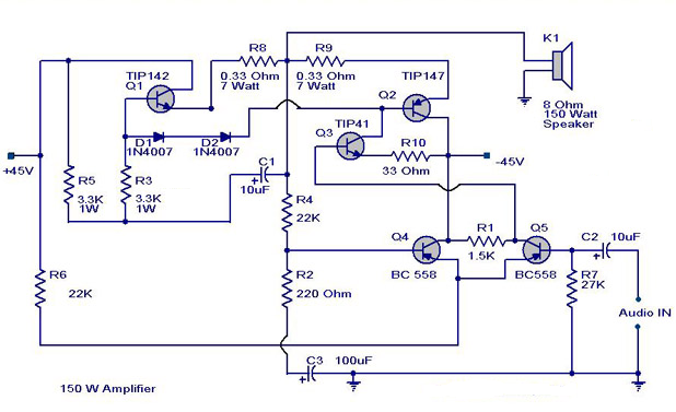
Notes.
- Remember TIP 142 and 147 are Darlington pairs .They are shown as conventional transistors in figure for ease.So don’t get confused.Even though each of them have 2 transistors ,2 resistors and 1 diode inside ,only three pins ,base emitter and collector are coming out.Rest are connected internally.So its quite OK to assume each of them as transistor for ease.
- Use a well regulated and filtered power supply.
- Connect a 10K POT in series with the input as volume control if you need.Not shown in circuit diagram.
- All electrolytic capacitors must be rated at least 50volts.
Power supply for this circuit.
A +40/-40 unregulated dual supply for powering this amplifier project is shown below. This power supply is only enough for powering one channel and for stereo applications double the current ratings of the transformer, diodes and fuses.
Wednesday, October 8, 2014
LM1877 bassed Audio power amplifier circuit and explanation
This audio amplifier circuit is designed to deliver 2W per channel continuous into 8Ω loads. The LM1877 is designed to operate with a low number of external components, and still provide flexibility for use in stereo phonographs, tape recorders and AM-FM stereo receivers, etc.
Each power amplifier is biased from a common internal regulator to provide high power supply rejection, and output Q point centering. The LM1877 is internally compensated for all gains greater than 10.
This audio amplifier circuit can be powered from a wide input voltage range from 6 volt up to 24 volts .
For this audio power amplifier circuit diagram you must use a 8 ohms speaker .
Friday, September 26, 2014
Simple Logarithmic Amplifier Circuit
For small input voltages, the amplification is high; when the input voltage rises, the amplification drops off and finally remains almost static for further increases in input voltage. Some applications of a logarithmic amplifier are: driving a graphic 4 recorder in weather stations, and in remote control systems (for instance, to avoid a too sudden and strong deflection of a servo arm). When used in conjunction with other equipment, the logarithmic amplifier is very flexible: analogue instruments as well as a row of LEDs can be connected to its output.
Operational amplifiers A1 and A2 form a non-inverting pre-amplifier. As the input signal of A3 should not under any circumstances be- come negative, the input level of the circuit can be shifted with potentiometer P1 as required. At the same time, this stage works as a high- impedance input buffer for A3. As shown, the amplifier accepts inputs up to 8 V. If a higher value ‘ is required, the amplification factors of Al and A2 can be suitably modified. l The logarithmic’ part of the circuit l consists of A3 and transistor array lC2: the voltage at pins 4 and 5 ~ of the array is related logarithmically with the output signal of A2.
The output stage of the circuit consists of amplifier A4 which amplifies the inverted signal from A3. As the amplification factor of this stage can be altered by l means of preset potentiometer P2, the output of the circuit can be matched to the load. To preset P2, connect a multimeter to the output of the circuit and a signal at maximum level to the input: adjust P2 to the required output voltage.

Tuesday, September 23, 2014
Automotive 12V to 20V converter for audio amplifier

The limitation of car supply voltage (12V) forces to convert the voltages to higher in order to power audio amplifiers.
In fact the max audio power x speaker (with 4 ohm impedance) using 12V is (Vsupply+ - Vsupply-)^2/(8*impedance) 12^2/32 = 4.5Watts per channel, that is laughable...
For powering correctly an amplifier the best is to use a symmetric supply with a high voltage differential. for example +20 - -20 = 40Volts
in fact
40^2/32 = 50 Watts per channel that is respectable.
This supply is intended for two channels with 50W max each (of course it depends on the amplifier used). Though it can be easily scaled up or the voltages changed to obtain different values.
Overview - How it works
It is a classic push-pull design , taking care to obtain best symmetry (to avoid flux walking). Keep in mind that this circuit will adsorb many amperes (around 10A) so take care to reinforce power tracks with lots of solder and use heavy wires from the battery or the voltage will drop too much at the input.
The transformer must be designed to reduce skin effect, it can be done using several insulated magnet wire single wires soldered together but conducting separately. The regulation is done both by the transformer turn ratio and varying the duty cycle. In my case i used 5+5 , 10+10 turns obtaining a step up ratio of 2 (12->24) and downregulating the voltage to 20 via duty cycle dynamic adjust performed by the PWM controller TL494.
The step-up ratio has to be a little higher to overcome diode losses, winding resistance and so on and input voltage drop due to wire resistance from battery to converter.
Transformer design
The transformer must be of correct size in order to carry the power needed, on the net there are many charts showing the power in function of frequency and core size for a given topology. My transformer size is 33.5 mm lenght, 30.0 height and 13mm width with a cross section area of 1,25cm^2, good for powers around 150W at 50khz.
The windings , especially the primary must be heavy gauged, but instead of using a single wire it is better to use
multiple wires in parallel each insulated from the other except at the ends. This will reduce resistance increase due to skin effect. The primary and secondary windings are centertapped, this means that you have to wind 5 turns, centertap and 5 windings again. The same goes for the secondary, 10 turns, centertap and 10 turns again.
The important thing is that the transformer MUST not have air gaps or the leakage inductance will throw spikes on the switches overheating them and giving a voltage higher than expected by turn ratio prediction, so if your voltage output (at fully duty cycle) is higher than Vin*N2/N1 - Vdrop diode, your transformer has gap (of course permit me saying you that you are BLIND if you miss it), and this is accompanied with a drastical efficiency reduction. Use non-gapped E cores or toroids (ferrite).
Output diodes, capacitors and filter inductor
For rectification i preferred to use shottky diodes since they have low forward voltage drop, and are incredibly fast.
I used the cheap 1N5822, the best alternative for low voltage converters (3A for current capability).
The output capacitors are 4700uF 25V, not very big, since at high frequency the voltage ripple is most due to internal cap ESR fortunately general purpose lytics have enough low esr for a small ripple (some tens of millivolts). Also at high duty cycle they are feed almost with pure DC, giving small ripple. The filter inductor on the secondary centertap furter increases the ripple and helps the regulation in asymmetrical transients
Power switch and driving
I used d2pak 70V 80A 0.004 ohms ultrafets (Fairchind semiconductor), very expensive and hard to find. In principle any fet will work, but the lower the on-resistance, the lower the on-state conduction losses, the lower the heat produced on the fets, the higher efficiency and smaller the heatsinks needed. With this fets i am able to run the fets with small heatsinks and without fan at full rated power (100W) with an efficiency of 82% and perceptible heating and with small heating at 120W (some degrees) (the core starts to saturate and the efficiency is a bit lower, around 75%)
Try to use the lowest resistance mosfet you can put your dirty hand :-) on or the efficiency will be lower than rated and you will need even a small fan. The fet driver i used is the TPS2811P, from Texas instruments, rated for 2A peak and 200ns. Is important that the gate drive is optimized for minimal inductance or the switching losses will be higher and you risk noise coupling from other sources. Personally i think that twisted pair wires (gate and ground/source) are the best to keep the inductance small. Place the gate drive resistor near the Mosfet, not near the IC.
Controller
I used the trusty TL494 PWM controller with frequency set at around 40-60 Khz adjustable with a potentiometer. I also implemented the soft start (to reduce powerup transients). The adjust potentiometer (feedback) must be set to obtain the desired voltage. The output signals is designed with two pull-up resistors on the collector of the PWM chip output transistor pulling them to ground each cycle alternatively. This signal is sent to the dual inverting MOSFET driver (TPS2811P) obtaining the correct waveform.
Power and filtering
How i said before the power tracks must be heavy gauged or you will scarify regulation (since it depends of transformer step up ratio and input voltage) and efficiency too. Dont forget to place a 10A (or 15A) fuse on the input because the car batteries can supply very high currents in case of shorts and this will save you face from a mosfet explosion in case of failture or short, remember to place a fuse also on the battery side to increase the safety (accidental shorts->fire, battery explosion, firemen, police and lawyers around). Input filtering is important, use at least 20000uF 16V in capacitors, a filter inductor would be useful too (heavygauged) but i decided to leave it..
Final considerations
This supply given me up to 85% efficiency (sometimes even 90% at some loads) with an input of 12V because i observed all these tricks to keep it functional and efficient. An o-scope would be useful, to watch the ripple and gate signals (watching for overshoots), but if you follow these guidelines you will avoid these problems.
The cross regulation is good but keep in mind that only the positive output is fully regulated, and the negative only follows it. Place a small load between the negative rail and ground (a 3mm led with a 4.7Kohm resistor) to avoid the negative rail getting lower then -20V. If the load is asymmetric you can have two cases:
-More load on positive rail-> no problems, the negative rail can go lower than -20V, but it is not a real issue for an audio amplifier.
-More load on negative rail-> voltage drop on negative rail (to ground) especially if the load is only on the negative rail.
Fortunately audio amplifiers are quite symmetrical as a load, and the output filter inductor/capacitors helps to maintain the regulation good during asymmetrical transients (Basses)
FOR FIRST TESTING USE A SMALL 12V power supply and use resistors as load monitoring switches heat and current consumption (and output) and try to determine efficiency, if it is higher then 70-75% you are set, it is enough. Adjust the frequency for best compromise between power and switching losses, skin effect and hysteresis losses
Bill Of Materials
=================
Design: 12V to 20V 100W DC-DC conv
Doc. no.: 1
Revision: 3
Author: Jonathan Filippi
Created: 29/04/05
Modified: 18/05/05
Parts
2 R1,R2 = 10
4 R3,R4,R6,R7 = 1k
1 R5 = 22k
1 R8 = 4.7k
1 R9 = 100k
2 C1,C2 = 10000uF
2 C3,C6 = 47u
1 C4 = 10u
3 C5,C7,C14 = 100n
2 C8,C9 = 4700u
1 C12 = 1n
1 C13 = 2.2u
1 U1 = TL494
1 U2 = TPS2811P
2 Q1,Q2 = FDB045AN
4 D1-D4 = 1N5822
1 D5 = 1N4148
1 FU1 = 10A
1 L1 = 10u
1 L2 = FERRITE BEAD
1 RV1 = 2.2k
1 RV2 = 24k
1 T1 = TRAN-3P3S
author: Jonathan Filippi
e-mail: jonathan.filippi@virgilio.it
web site: http://www.cool-science.tk
Monday, September 22, 2014
Automotive 12V to 20V converter for audio amplifier descriptiona and circuit diagram
Circuit diagrams
The limitation of car supply voltage (12V) forces to convert the voltages to higher in order to power audio amplifiers.
In fact the max audio power x speaker (with 4 ohm impedance) using 12V is (Vsupply+ - Vsupply-)^2/(8*impedance) 12^2/32 = 4.5Watts per channel, that is laughable...
For powering correctly an amplifier the best is to use a symmetric supply with a high voltage differential. for example +20 - -20 = 40Volts
in fact
40^2/32 = 50 Watts per channel that is respectable.
This supply is intended for two channels with 50W max each (of course it depends on the amplifier used). Though it can be easily scaled up or the voltages changed to obtain different values.
Overview - How it works
It is a classic push-pull design , taking care to obtain best symmetry (to avoid flux walking). Keep in mind that this circuit will adsorb many amperes (around 10A) so take care to reinforce power tracks with lots of solder and use heavy wires from the battery or the voltage will drop too much at the input.
The transformer must be designed to reduce skin effect, it can be done using several insulated magnet wire single wires soldered together but conducting separately. The regulation is done both by the transformer turn ratio and varying the duty cycle. In my case i used 5+5 , 10+10 turns obtaining a step up ratio of 2 (12->24) and downregulating the voltage to 20 via duty cycle dynamic adjust performed by the PWM controller TL494.
The step-up ratio has to be a little higher to overcome diode losses, winding resistance and so on and input voltage drop due to wire resistance from battery to converter.
Transformer design
The transformer must be of correct size in order to carry the power needed, on the net there are many charts showing the power in function of frequency and core size for a given topology. My transformer size is 33.5 mm lenght, 30.0 height and 13mm width with a cross section area of 1,25cm^2, good for powers around 150W at 50khz.
The windings , especially the primary must be heavy gauged, but instead of using a single wire it is better to use
multiple wires in parallel each insulated from the other except at the ends. This will reduce resistance increase due to skin effect. The primary and secondary windings are centertapped, this means that you have to wind 5 turns, centertap and 5 windings again. The same goes for the secondary, 10 turns, centertap and 10 turns again.
The important thing is that the transformer MUST not have air gaps or the leakage inductance will throw spikes on the switches overheating them and giving a voltage higher than expected by turn ratio prediction, so if your voltage output (at fully duty cycle) is higher than Vin*N2/N1 - Vdrop diode, your transformer has gap (of course permit me saying you that you are BLIND if you miss it), and this is accompanied with a drastical efficiency reduction. Use non-gapped E cores or toroids (ferrite).
Output diodes, capacitors and filter inductor
For rectification i preferred to use shottky diodes since they have low forward voltage drop, and are incredibly fast.
I used the cheap 1N5822, the best alternative for low voltage converters (3A for current capability).
The output capacitors are 4700uF 25V, not very big, since at high frequency the voltage ripple is most due to internal cap ESR fortunately general purpose lytics have enough low esr for a small ripple (some tens of millivolts). Also at high duty cycle they are feed almost with pure DC, giving small ripple. The filter inductor on the secondary centertap furter increases the ripple and helps the regulation in asymmetrical transients
Power switch and driving
I used d2pak 70V 80A 0.004 ohms ultrafets (Fairchind semiconductor), very expensive and hard to find. In principle any fet will work, but the lower the on-resistance, the lower the on-state conduction losses, the lower the heat produced on the fets, the higher efficiency and smaller the heatsinks needed. With this fets i am able to run the fets with small heatsinks and without fan at full rated power (100W) with an efficiency of 82% and perceptible heating and with small heating at 120W (some degrees) (the core starts to saturate and the efficiency is a bit lower, around 75%)
Try to use the lowest resistance mosfet you can put your dirty hand :-) on or the efficiency will be lower than rated and you will need even a small fan. The fet driver i used is the TPS2811P, from Texas instruments, rated for 2A peak and 200ns. Is important that the gate drive is optimized for minimal inductance or the switching losses will be higher and you risk noise coupling from other sources. Personally i think that twisted pair wires (gate and ground/source) are the best to keep the inductance small. Place the gate drive resistor near the Mosfet, not near the IC.
Controller
I used the trusty TL494 PWM controller with frequency set at around 40-60 Khz adjustable with a potentiometer. I also implemented the soft start (to reduce powerup transients). The adjust potentiometer (feedback) must be set to obtain the desired voltage. The output signals is designed with two pull-up resistors on the collector of the PWM chip output transistor pulling them to ground each cycle alternatively. This signal is sent to the dual inverting MOSFET driver (TPS2811P) obtaining the correct waveform.
Power and filtering
How i said before the power tracks must be heavy gauged or you will scarify regulation (since it depends of transformer step up ratio and input voltage) and efficiency too. Dont forget to place a 10A (or 15A) fuse on the input because the car batteries can supply very high currents in case of shorts and this will save you face from a mosfet explosion in case of failture or short, remember to place a fuse also on the battery side to increase the safety (accidental shorts->fire, battery explosion, firemen, police and lawyers around). Input filtering is important, use at least 20000uF 16V in capacitors, a filter inductor would be useful too (heavygauged) but i decided to leave it..
Final considerations
This supply given me up to 85% efficiency (sometimes even 90% at some loads) with an input of 12V because i observed all these tricks to keep it functional and efficient. An o-scope would be useful, to watch the ripple and gate signals (watching for overshoots), but if you follow these guidelines you will avoid these problems.
The cross regulation is good but keep in mind that only the positive output is fully regulated, and the negative only follows it. Place a small load between the negative rail and ground (a 3mm led with a 4.7Kohm resistor) to avoid the negative rail getting lower then -20V. If the load is asymmetric you can have two cases:
-More load on positive rail-> no problems, the negative rail can go lower than -20V, but it is not a real issue for an audio amplifier.
-More load on negative rail-> voltage drop on negative rail (to ground) especially if the load is only on the negative rail.
Fortunately audio amplifiers are quite symmetrical as a load, and the output filter inductor/capacitors helps to maintain the regulation good during asymmetrical transients (Basses)
FOR FIRST TESTING USE A SMALL 12V power supply and use resistors as load monitoring switches heat and current consumption (and output) and try to determine efficiency, if it is higher then 70-75% you are set, it is enough. Adjust the frequency for best compromise between power and switching losses, skin effect and hysteresis losses
Bill Of Materials
=================
Design: 12V to 20V 100W DC-DC conv
Doc. no.: 1
Revision: 3
Author: Jonathan Filippi
Created: 29/04/05
Modified: 18/05/05
Parts
2 R1,R2 = 10
4 R3,R4,R6,R7 = 1k
1 R5 = 22k
1 R8 = 4.7k
1 R9 = 100k
2 C1,C2 = 10000uF
2 C3,C6 = 47u
1 C4 = 10u
3 C5,C7,C14 = 100n
2 C8,C9 = 4700u
1 C12 = 1n
1 C13 = 2.2u
1 U1 = TL494
1 U2 = TPS2811P
2 Q1,Q2 = FDB045AN
4 D1-D4 = 1N5822
1 D5 = 1N4148
1 FU1 = 10A
1 L1 = 10u
1 L2 = FERRITE BEAD
1 RV1 = 2.2k
1 RV2 = 24k
1 T1 = TRAN-3P3S
author: Jonathan Filippi
e-mail: jonathan.filippi@virgilio.it
web site: http://www.cool-science.tk
Saturday, September 20, 2014
700W Leach Amplifier

Technical parameters:
Output: 680W/2R, 450W/4R, 260W/8R
Minimum speaker impedance: 2R
Bandwidth: 10-180 000Hz/-3dB
Maximum permissible voltage: max + /-80V
Fusing end amplifier: 2x 15A / F
Late connection: approx 1.5 sec
Input sensitivity for maximum excitation: 1.1 V
Slew rate: 35V/us


STK4050 Audio Amplifier with 200W Output
Friday, September 19, 2014
TDA1566 Audio Amplifier 2x46W 1x92W
TDA1566general description:
TDA1566 features:
- Operates in I2C-bus mode and non-I2C-bus mode
- TH version: four I2C-bus addresses controlled by two pins; J version: two I2C-busaddresses controlled by one pin
- Two 4 Ω or 2 Ω capable BTL channels or one 1 Ω capable BTL channel
- Low offset
- Pop free off/standby/mute/operating mode transitions
- Speaker fault detection
- Selectable gain (26 dB and 16 dB)
- In I2C-bus mode:
- DC load detection: open, short and speaker or line driver present
- AC load (tweeter) detection
- Programmable trigger levels for DC and AC load detection
- Per channel programmable gain (26 dB and 16 dB, selectable per channel)
- Selectable diagnostic levels for clip detection and thermal pre-warning
- Selectable information on the DIAG pin for clip information of each channelseparately and independent enabling of thermal-, offset- or load fault
- Independent short-circuit protection per channel
- Loss of ground and open VP safe
- All outputs short-circuit proof to VP, GND and across the load
- All pins short-circuit proof to ground
- Temperature controlled gain reduction at high junction temperatures
- Fault condition diagnosis per channel: short to ground, short to supply, shorted leadand speaker fault (wrongly connected)
- Low battery voltage detection
- TH version: pin compatible with the TDA8566TH1
TDA1566 circuit:
 |
| TDA1566 Audio Amplifier 2x46W |
 |
| TDA1566 Audio Amplifier 2x46W |
TDA1566 layout:
 |
| TDA1566 Audio Amplifier 2x46W layout |
 |
| TDA1566 Audio Amplifier 2x46W pcb |
 |
| TDA1566 Audio Amplifier 2x46WTDA1566 Audio Amplifier 2x46W pcb |
 |
| TDA1566 Audio Amplifier 2x46W pcb |
18 W stereo amplifier circuit
TDA1009 circuit amplifier , this circuit is stereo amplifier and simple schematic .Minimum voltage require 9V and maximum voltage 24V. To avoid damaged IC please use supply voltage 12 volt and must be filtering voltage. Power output 2 X 18 W with impedance 4 Ohm.See circuit schematic and troubleshooting amplifier :
 |
| Click to view larger |
- Supply voltage.
- Components damaged , such as IC , resistor ,and Capacitor.
- Installation components inverted.
- Broken line PCB.
- Input not connected. Or input grounding.
- Output Not connected.
- Speakers damaged.
Thursday, September 18, 2014
Strong Headphone Amplifier
Strong Headphone Amplifier Circuit diagram:
Parts:
Resistors:
P1 = 22K Potentiometer
R1 = 15K Resistor
R2 = 100K Resistor
R3 = 100K Resistor
R4 = 47K Resistor
R5 = 470R Resistor
R6 = 500R Resistor
R7 = 1K Resistor
R8 = 18K Resistor
R9 = 18K Resistor
R10 = 2.2R Resistor
R11 = 2.2R Resistor
R12 = 33R Resistor
R13 = 4.7K Resistor
Capacitors:
C1 = 10uF-25V Capacitors
C2 = 10uF-25V Capacitors
C3 = 100nF-63V (PF)
C4 = 220uF-25V Capacitors
C5 = 100nF-63V (PF)
C6 = 220uF-25V Capacitors
Semiconductors:
Q1 = BC560C PNP Transistor
Q2 = BC560C PNP Transistor
Q3 = BC550C NPN Transistor
Q4 = BC550C NPN Transistor
Q5 = BC560C PNP Transistor
Q6 = BC327 PNP Transistor
Q7 = BC337 NPN Transistor
Miscellaneous:
J1 = RCA Audio Input Socket
J2 = 3mm Stereo Jack Socket
B1 = 6V Battery Rechargeable
SW1=SPST Slide or Toggle Switch
Notes:
- For a Stereo version of this schema, all parts must be doubled except P1, SW1, J2 and B1.
- Before setting quiescent current rotate the volume control P1 to the minimum, Trimmer R6 to maximum resistance and Trimmer R3 to about the middle of its travel.
- Connect a suitable headphone set or, better, a 33 Ohm 1/2W resistor to the amplifier output.
- Switch on the supply and measure the battery voltage with a Multimeter set to about 10Vdc fsd.
- Connect the Multimeter across the positive end of C4 and the negative ground.
- Rotate R3 in order to read on the Multimeter display exactly half of the battery voltage previously measured.
- Switch off the supply, disconnect the Multimeter and reconnect it, set to measure about 10mA fsd, in series to the positive supply of the amplifier.
- Switch on the supply and rotate R6 slowly until a reading of about 3mA is displayed.
- Check again the voltage at the positive end of C4 and readjust R3 if necessary.
- Wait about 15 minutes, watch if the current is varying and readjust if necessary.
- Those lucky enough to reach an oscilloscope and a 1 KHz sine wave generator can drive the amplifier to the maximum output power and adjust R3 in order to obtain a symmetrical clipping of the sine wave displayed.
Technical data:
Output power (1 KHz sine wave):
- 16 Ohm: 100mW RMS
- 32 Ohm: 60mW RMS
- 64 Ohm: 35mW RMS
- 100 Ohm: 22.5mW RMS
- 300 Ohm: 8.5mW RMS
- 160mV input for 1V RMS output into 32 Ohm load (31mW)
- 200mV input for 1.27V RMS output into 32 Ohm load (50mW)
- Flat from 45Hz to 20 KHz, -1dB @ 35Hz, -2dB @ 24Hz
- 1V RMS (62mW) 0.015% 1.27V RMS (onset of clipping, 100mW) 0.04%
- 1V RMS (62mW) 0.05% 1.27V RMS (onset of clipping, 100mW) 0.1%
- Unconditionally stable on capacitive loads
Monday, September 15, 2014
Stereo Power Amplifier Using IC 7905
Circuit diagram :
Saturday, September 13, 2014
Improving Performance Bass Amplifier
If still, you need to use 2 power supply or attempting to use this circuit. Note this circuit works for a power amp that is less power transformer with 2 speakers (stereo). One of the speaker cable (output) should be reversed, this is okay, just a game to lighten the work phase transformer from the blow bass.
List of components:
R1, 2,5,6 .......... 100K
R3, 4 ................ 2K2
R7 ................... 100
R9, 10 .............. 2K2-3K3
C1, 2 ............... 100uf/25V
D1, 2 ............... 15V Zener
IC1 ................. TL072
