Showing posts with label using. Show all posts

Tuesday, November 11, 2014

Long Duration Timer using ATtiny2313

This timer circuit is designed to switch on a 12 V load in a solar-powered installation for a preset period at the press of a button. When the period has expired a latching relay disconnects both the load and the controller circuit from the 12 V supply. The length of the period can be configured by making suitable changes to the microcontroller’s source code.
When button S1 is pressed a voltage appears across relay coil L1, and the relay switches the load on. Since the relay is a latching type, it remains in this state when the but ton is released. There is now a supply to the 78L05 voltage regulator (a low-dropout type such as the LP2950CZ-5.0 may also be used) and the microcontroller is powered up. In the microcontroller the timer program runs until the configured time interval has elapsed. Around 90 % of the way through the time period LED D2 lights as a warning that the load will shortly be switched off, and this time can also of course be configured by changing the software.

When the full time interval has elapsed the microcontroller sets an output (pin 7) high, which triggers the CNY 17-3 optocoupler and in turn drives relay coil L2. The relay returns to its initial state, disconnecting the load as well as the controller (which is also powered via the relay contact) from the 12 V supply.Long Duration Timer Circuit Diagram

The author used a miniature 16 -by-2 LCD panel type HMC16223SG in his prototype, measuring just 52 mm by 20 mm. It is of course possible to use any standard LCD module that uses an HD44780-compatible controller. Note that P1 is used to adjust the contrast of the LCD: if the display appears blank it is worth checking the contrast set-ting before suspecting a more serious problem! If desired, the LCD can be dispensed with, along with the corresponding parts of the source code.

The upper line of the LCD shows the total time period, in seconds, for which the soft-ware is configured, while the lower line shows the time, in seconds, since the button was pressed.

The screendump shows the LCD settings under BASCOM-AVR.  
Read More..

Thursday, October 9, 2014

Circuit Switching Regulators Using LM2575 and LM2577

Switching regu­lators are available is different circuit configurations in­cluding the flyback, feed-forward, push-pull, and non-iso­lated single-ended or single-polarity types. Also, the switching regulators can operate in any of three modes – step-down, step-up, or polarity inverting.
rovide the active functions for step-down (back) switching regulator, capable of driving a1A load with excellent line and load regulation. These devices are available in fixed output voltages of 3.3V, 5V, 12V, 15V and an adjustable output version.

Requiring a minimum number of external components, these regulators are simple to use and include internal frequency compensation and a fixed-frequency oscillator. LM 2575 series offers a high-efficiency replacement for popular 3-terminal linear regulators. It substantially reduces the size of the heat sink, and in many cases no heat sink is required. Fixed output voltage version is illustrated in figure.

The National Semiconductor LM 1577/LM 2577 are monolithic ICs that provide all of the power and control functions for step-up (boost), fly back, and forward converter switching regulators. The device is available in three different output voltage versions: 12 V, 15 V and adjustable.

Read More..

Wednesday, October 8, 2014

Low Cost Fire Alarm Circuit and explanation Using Transistor

Transistor BC177 (Q1) is used as the fire sensor here. When the temperature increases the leakage current of this transistor also increases.The circuit is designed so that when there is an increase in the leakage current of Q1, transistor Q2 will get biased. As a result when there is a fire breakout the transistor Q2 will be on. The emitter of Q2 (BC 108)is connected to the base of Q3(AC 128). So when Q2 is ON Q3 will be also ON. The transistor Q3 drives the relay which is used to drive the load ie,light,bell,horn etc as an indication of the fire. The diode D1 is used as a free wheeling diode to protect it from back EMF generated when relay is switched.


Notes:
  • The Preset R1 can be used to desired temperature level for setting the alarm ON.
  • This is not a latching alarm,ie; when the temperature in the vicinity of the sensor decreases below the set point the alarm stops.
  • The circuit can be powered using a 9V battery or a 9V battery eliminator.
  • All capacitors are electrolytic and must be rated at least 10V.
  • The load can be connected through the C,NC,NC points of the relay according to your need.
  • The calibration can be done using a soldering iron,and a thermo meter. Switch ON the power supply.Keep the tip of soldering iron near to the Q1.Same time also keep the thermometer close to it.When the temperature reaches your desired value adjust R1 so that relay gets ON.
Read More..

Friday, October 3, 2014

Ramp Generator Circuit using NE555

We know that if a capacitor is charged from a voltage supply through a resistor, an exponential waveform is created while charging of a capaci­tor from a continuing current supply produces a ramp. this is the concept behind the circuit. The circuit of a ramp generator using timer 555 is shown in figure. Here the resistor of previ­ous circuits is replaced by a PNP transistor that produces a continuing charging current.

Charging current produced by PNP constant current source is

iC = Vcc-VE / RE

where VE = R2 / (R1 + R2) * VCC + VBE

When a trigger starts the monostable multivibrator timer 555 as shown in figure, the PNP current supply forces a continuing charging into the capacitor C. The voltage across the capacitor is, therefore, a ramp as illustrated in the figure. The slope of the ramp is given as Slope, s = I/C

Read More..

Friday, September 26, 2014

Lamp Flasher Circuit Using Thermistors

A simple very low frequency oscillator or flasher circuit can be made by interconnecting one positive temperature co-efficient and one negative temperature co-efficient thermistor in series.
For conditions of oscillation the characteristics of the two devices have to be chosen carefully. The operating point is determined by the intersection of the two curves.

Read More..

Thursday, September 25, 2014

Electronic Voltmeter Ammeter Circuit Using Single IC 741

Simple Electronic Multimeter  High cost deters many hobbyists from buying a conventional multimeter. Since it is difficult to obtain cheap 50 uAor 100uA meters which are essential for a highly sensitive multimeter, an electronic alternative device is suggested to serve the purpose. The circuit shown here gives economic and safe ranges covered to three values : (i) 0-15V, (ii) 0- l5mA, and (iii) 0-150mA.
The ranges can be extended with suitable modifications. The 741 operational amplifier acts as a null detector. its output is equal to the voltage at point A minus the voltage at , point B, multiplied by the device’s very high voltage gain. lf VA is slightly greater than VB, the output is limited by the supply voltage to about 7 volts. lf  VA is slightly less than VB, the output is about 2 volts. At the point at which the output changes from low to high or vice-versa, VA is equal to VB to within a very small margin of error. With the switch set to the position shown in circuit diagram (15V range) the potential difference between points A and C is

R3+R4+R5/R1+R2+R3+R4+R5 * input voltage

or 1/30 * input voltage


 The forward voltage drop of the diode D3 is about 0.6V and largely independent of battery condition. About 0.5V appears across the variable resistance VRl and a known fraction of this indicated by a scale on the potentiometer appears between points A and C, i.e. it compares the known reference voltage with a known fraction of the input voltage. On the two current ranges, the reference potential difference is compared with the voltages developed across R4 plus R5 on the l5mA range and R5 only in 150mA range. T D2, a light emitting diode, with its current limiting series resistor R9 indicates whether the output of the operational amplifier is high or low. The diode D1 and the condenser Cl provide the facility of measuring alternating voltages and  currents. lf the voltage at A momentarily exceeds the voltage at B, then Cl will charge up via Dl maintaining D2»alight until the peak of the next cycle. Without Cl there is no sharp point at which D2 extinguishes for AC measurement. ln use it must be remembered that the indicated readings are all peak values and will thus need to be divided by square-root of 2 to give RMS value for a sinusoidal input. The meter is calibrated directly VRl is scaled 0-15 on the _ 15V range by comparison with a standard meter. This calibration will hold quite closely for current ranges—the agreement depending on the tolerances of Rl to R5. Ten per cent tolerance resistors have been found to be quite successful for these but, if desired, 5 or even 2 per cent resistors provide a worthwhile increase in the accuracy of the current ranges. ln use, the meter is switched to the appropriate range and V connected as for a conventional multimeter. The potentiometer VR] is rotated until D2 is at the point of changing from off to on and then the reading is directly indicated. on the potentiometer scale. The diodes may be any silicon diode. For use of the multimeter in 0- l 50V range, the values of the resistors Rl to R5 may be changed proportionately so that the value of the ratio

R3+R4+R5/R1+R2+R3+R4+R5

is l/300. Then with these values, the multimeter will operate on 0- l 5OV range in the first position (as shown in the existing diagram). The accuracy no doubt will be somewhat ham- pered. VRl has to be calibrated accordingly.

Electronic voltmeter, ammeter circuit using a single IC 741

Read More..

Monday, September 15, 2014

Stereo Power Amplifier Using IC 7905

79xx is a widely known series of low-cost, fixed-negative-voltage regulators. These integrated diagram are available with output current of 100-150 mA (L series), 0.4-0.5A (M series), up to 1A (standard series), etc. They can be used in many applications other than regulators, audio power amplifier being one of them.  As shown in the schema diagram, a simple stereo audio amplifier is built around two 7905 negative-voltage regulators (IC1 and IC2) and a few discrete components. The 7905 IC (a -5V regulator) used here is readily available. However, the schema will also work with other 79XX regulators if appropriate power supply is used. Both channels shown in the diagram are identical. Hence the description below is only for the first channel. The quality of the output signal is within acceptable limits. 

Circuit diagram :
Stereo-Power-Amplifier
Stereo Power Amplifier Circuit Diagram
 
Regulator IC 7905 works as an amplifier for the voltages applied to common pin2 (Ground or GND). The minimal voltage drop over the standard 7905 is around 2V and it depends on the output current. Feedback resistors in the IC set the gain of the channel internally. The amplifier is a class-A audio amplifier. The regulator IC produces the negative output signal. 

Resistor R3 provides the positive signal. It limits the maximum output current of the regulator during the negative half period of the amplified sinusoidal signal. The minimal applicable value of R3 for the regulator 7905 is 8.2 to 10 ohms per 5W.  Optimisation of the value of R3 depends on the output voltage of the regulator, negative power supply (–5V) and load resistance of loudspeaker (LS1). If the required output current for LS1 is below 100 mA, the value of resistor R3 can be 33 to 51 ohms per watt. 

Normally, the load resistance of the loudspeaker should be higher than of R3 in order to obtain a large peak-to-peak amplitude. But this can be neglected in order to obtain lower power dissipation on R3 and the IC. The schema works with any load resistance (R3 in parallel with LS1 as the load) under the condition that the regulator is not overloaded with current and power dissipation. However, it is preferable to use a loudspeaker with a high resistance (8 ohms, 16 ohms or more). The amplifier works well with low-impedance headphones having a resistance of 24 to 32 ohms. The voltage difference between the ground pin of 7905 and the output pin is fixed internally. 

The input resistance of the amplifier is relatively low and depends on potentiometer VR1 and input resistance of the ground pin. Practically, any stereo output capable of driving 24- or 32-ohm headphones and loudspeakers can drive the input of the stereo amplifier with 7905. If VR1 is removed, the amplifier will still work but there will be more distortion. Therefore potentiometer VR1 is used to provide sufficient variable audio signal.  The values of output capacitors C10 and C11 are usually between 0.1 µF and 1 µF. A small resistance can be connected in series with them if needed. S2 is the on/off switch. Switch S1 is for mono/stereo selection. When switch S1 is closed, the amplifier works as a two-way mono amplifier. If S1 is open, the amplifier works as a stereo amplifier. 

The schema is powered by a 12V battery. The positive terminal of the battery is the common node. The negative terminal is connected to pin 2 of IC1, which is the –12V supply line. The maximum operating voltage can be up to –35V. If no input signal is applied, the DC voltage on the output of the regulator 7905 should be around –5V, which depends to some extent on the value of VR1. The maximum output current of 7905 can be up to 1A and the maximum power dissipation is up to 15W. IC 7905 has internal thermal protection. 

Assemble the schema on a general-purpose PCB and enclose in a suitable cabinet. Fix the stereo female jack on the front panel and speaker to the rear side of the cabinet, and the 12V battery inside the cabinet. Fix LED1 and switches S1 and S2 too on the front panel of the cabinet. Mount the regulator IC 7905 on a heat-sink with thermal resistance below 15°C/W. The metallic part on the case is internally connected with the input pin of the regulator.

Author : Petre tzv. Petrov Sourced by: EFy
Read More..

Wednesday, September 10, 2014

Simple Subwoofer Lowpass Filter using uA741 Single Op Amp Ic

This is the simplest Sub woofer Low Pass filter Circuit using uA741 single op amp ic. The schema is very low cost with respect to their work. The cut off frequency of this schema is 25Hz to 80Hz maximum. Using this schema , you can easily design a 2.1 Sub-woofer Speaker System at your own Home. The schema contains very few components.In Pakistan, the cost of this schema with PCB is Rs:45 The same schema is working in my own hand made sub-woofer system. So Try this [Link]

Lowpass

Parts List: 

R1,R3,R4 = 10K 1/4W
R2=100K 1/4W
CY1,CY2 = 0.22uF Polyester
C1,C2 = 10uF/25V Electrolytic
IC1 = uA741A Single Op-Amp Ic + 8 Pin Ic Socket
3 Pin Male & Female Connector x 2
2 Pin Male & Female Connector x 1
PCB as in required size 4.5 cm x 3.4 cm
Read More..

Wednesday, August 27, 2014

9 Volt Power Supply Wiring diagram Schematic Using IC 7809

Description
Circuit showing a 9 volt power supply . Here we have used a bridge rectifier and 7809 ic for making this schema.Where the ic regulate the output to 9 v,1 A .This voltage every time constant.Are you interested ?

Circuit diagram with Parts list. 


Notes. 
  • If a current of 300 mA or above is required, fit a proper heat sink to the IC 7809.
  • If 1A bridge is not available, make one using four 1N 4007 diodes.
Read More..

Wednesday, August 20, 2014

7 segment rolling display using PC


It is very interesting and convenient to be able to control everything while sitting at your PC terminal. Here, a simple hardware schema and software is used to interface a 7-segment based rolling display. The printer port of a PC provides a set of points with some acting as input lines and some others as output lines.


http://www.electronic-diagram-diagrams.com/computersimages/4.gif


Some lines are open collector type which can be used as input lines. The schema given here can be used for interfacing with any type of PC’s printer port. The 25-pin parallel port connector at the back of a PC is a combination of three ports. The address varies from 378H-37AH. The 7 lines of port 378H (pins 2 through 8) are used in this schema to output the code for segment display through IC1. The remaining one line of port 378H (pin 9) and four lines of port 37AH (pins 1, 14, 16, 17) are used to enable the display digits (one a time) through IC2. The bits D0, D1 and D3 of port 37AH connected to pins 1, 14 and 17 of ‘D’ connector are inverted by the computer before application to the pins while data bit D2 is not inverted. Therefore to get a logic high at any of former three pins, we must send logic 0 output to the corresponding pin of port 37AH. Another important concept illustrated by the project is the time division multiplexing. Note that all the five 7-segment displays share a common data bus. The PC places the 7-segment code for the first digit/character on the data bus and enables only the first 7-segment display. After delay of a few milliseconds, the 7-segment code for the digit/character is replaced by that of the next charter/digit, but this time only second display digit is enabled. After the display of all characters/digits in this way, the cycle repeats itself over and over again. Because of this repetition at a fairly high rate, there is an illusion that all the digits/characters are continuously being displayed. DISP1 is to be physically placed as the least significant digit. IC1 (74LS244) is an octal buffer which is primarily used to increase the driving capability. It has two groups of four buffers with non-inverted tri-state outputs. The buffer is controlled by two active low enable lines. IC2 (75492) can drive a maximum of six 7-segment displays. (For driving up to seven common-cathode displays one may use ULN2003 described elsewhere in this section.) The program for rolling display is given in the listing DISP.C above. Whatever the message/characters to be displayed (here five characters have been displayed), these are separated and stored in an array. Then these are decoded. Decoding software is very simple. Just replace the desired character with the binary equivalent of the display code. The display code is a byte that has the appropriate bits turned on. For example, to display character ‘L’, the segments to be turned on are f, e and d. This is equivalent to 111000 binary or 38 hex. Please note that only limited characters can be formed using 7-segment display. Characters such as M, N and K cannot be formed properly

Read More..

Wednesday, August 13, 2014

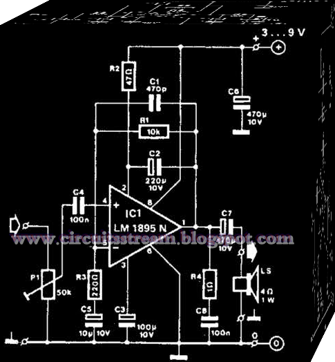
Using Lm1895N Mini Amplifier Wiring diagram Schematic

 This is an IC Based Amplifier schema. This is Using Lm1895N Mini Amplifier Circuit Diagram. This schema with 3-V to 9-V supplies, this amplifier can provide from 100-mW to 1-W output into a 4 and bandwidth is approximately 20 kHz @ 3 dB. This schema is useful for low-power and battery applications. Drain is 80 mA @ 3 V or 270 mA @ 9 V at maximum signal conditions.

Using Lm1895N Mini Amplifier Circuit Diagram


using Lm1895N Mini Amplifier Circuit Diagram
Read More..